SlideShare a Scribd company logo
UNIT 3
I/O INTERFACING
Memory Interfacing and I/O interfacing - Parallel
communication interface – Serial communication interface
8/I;– D/A and A/D Interface – Interrupt controller –
Programming and applications Case studies: Traffic Light
control, LED display and LCD display.
CO- Explain how peripherals (8255, 8253, etc.) are
interconnected with the microprocessor
8086 microprocessor -Input/Output INTERFACING
. Input port : used to read the data from key board
Tri state buffer is used as the Input port.
Its output is available only when its enable line
is active
Output port : send the data to the printer or display
Latches are used as the Output port
Output is available only when its enable line is active
 Several memory chips(ROM, RAM) or I/O devices (key board, display, printer) are
connected to a microprocessor.
 An address decoding circuit(decoder/demultiplexer) is used to select the required
I/O device or a memory chip.
 transfer of data between I/O devices and the microprocessor is called as I/O data
transfer
 This data transfer takes place through I/O port
Components used for Memory or I/O interfacing
are decoder/demultiplexer, tri-state buffer, latches
I/O Interfacing
Steps in Interfacing an I/O Device
The following steps are performed to interface a general I/O device with a CPU:
1. Connect the data bus of the microprocessor system with the data bus of the I/O port.
2. Derive a device address pulse by decoding the required address of the device and use it as the
chip select of the device.
3. Use a suitable control signal, IORD and/or IOWR to carry out device operations, i.e. connect
IORD to RD input of the device if it is an input devise, otherwise connect IOWR to WR input of
the device. In some cases the RD or WR control signals are combined with the device address
pulse to generate the device select pulse.
I/O Interfacing
Memory organization in 8086
BHE and Ao are used for decoding
the required chip select signals for
the odd and even memory banks
Memory and I/o devices are interfaced with the micro processor in two ways
1. Memory mapped I/O
2. I/O mapped I/O
When = 1, memory operation takes place
= 0, I/O operation takes place
8086 microprocessor -Input/Output INTERFACING
Parallel communication interface
 8255 is a programmable peripheral interface(PPI) device designed to interface the
microprocessor with its outside world such as ADC, DAC, keyboard etc.
 It can be programmed to transfer data under various conditions
INTEL 8255- programmable peripheral interface(PPI)
•PA0 – PA7 – Pins of port A
•PB0 – PB7 – Pins of port B
•PC0 – PC7 – Pins of port C
•D0 – D7 – Data pins for the transfer of
data (connected to 8086 data lines)
•RESET – Reset input
•RD’ – Read input
•WR’ – Write input
•CS’ – Chip select
•A1 and A0 – Address pins
 It consists of 40 pins and operates in
+5V regulated power supply.
PIN diagram
It consists of three 8-bit bidirectional I/O ports( 24 lines) through which the input,
output devices are connected.
1. PORT A
2. PORT B
3. PORT C.
Port C is further divided into two 4-bit ports i.e. port C lower and port
C upper and port C
I/O ports
 Each port has unique address and data to read/write
The pins A0, A1 will select the ports which is to be connected to the D0 to D7
CS’ – Chip select lines used to select the 8255, since multiple 8255 are connected
When CS’ =0, that particular 8255 is selected
Selection of port(commands to control blocks)
When A0, A1=00, port A is selected
=01 , port B is selected
=10 , port C is selected
=11, control register is
selected for programming
As soon as we connect 8255, we can
program using control register
Internal Block diagram of 8255
 This unit accepts control signals ( RD’, WR’ ) and also inputs from address(A1, A0)
bus and issues commands to control blocks .
 It has the following pins.
CS’ , RD’ , WR’ , RESET , A1 , A0
RESET : The 8255 is placed into its reset state if this input line is a logical 1
 This is a tristate bidirectional buffer used to interface 8255 to microprocessor system
data bus.
 Data is transmitted or received by the buffer on execution of input or output
instruction by the microprocessor.
1. Data bus buffer
2. Read/Write control logic
 These block receive control from the microprocessor and issues commands to their
respective ports.
 2 groups of control blocks are present
 Group A [Port-A (PA) & Port C Upper PCU(PC7 –PC4)]
consist of port A and port C upper.
 Group B [Port-B (PB )& Port C Lower PCL ( PC3 –PC0)]
consists of port C lower and port B
3. Control block
Modes of operation of 8255
1. Bit set/Reset (BSR) mode
The BSR mode is used to set or reset the bits in port C.
2. I/O mode.
The I/O mode is further divided into 3 modes:
(i) mode 0 : all ports function as simple Input/output
 Each of the port will work independently. Port A, Port B can be configured
as simple 8 bit Input/output port without handshaking.
 Two halves of Port C together work as 8 bit port or Port C as two 4-bit
ports
(ii) mode 1 I/O with handshake
 Group A consist of port A (8 bit) and upper half of port C (4 bit) and
Group B consist of port A (8 bit) and lower half of port C (4 bit)
 port A and port B can be programmed as 8 bit input or output ports with 4
lines of port C in each group is used for handshaking
(iii) mode 2 Bidirectional data transfer
 Only port A can be used as bidirectional port.
 Handshaking signals are provided on five lines of port C(PC3 –PC7)
Two primary modes
8255 has 8 bit control register
8255 ports can be configured for operation by writing appropriate control word
When A0, A1=11, control register is used for programming by setting the control word
control register
control word format
For parallel I/O
When D7=1, the word loaded into the control register is a mode definition word
D7=0, it is taken as a bit set or reset word
Appropriate words are set or reset depends on the type of operation desired, and loaded
into the control register
Control words defines the complete function of PPI.
They are loaded before any transmission or reception
For BSR mode
S/R = 1 for set
=0 for reset
 Depending upon the value if CS’, A1 and A0 we can select different ports in
different modes as input-output function or BSR.
 This is done by writing a suitable word in control register (control word D0-D7).
8086 microprocessor -Input/Output INTERFACING
Basics of serial communication
Transmitter:
- A parallel-in, serial-out shift register
Receiver:
- A serial-in, parallel-out shift register.
In parallel transmission, number of data lines depends on number of bits to be transmitted
For long distance communication, parallel transmission is impractical(increase in cost)
a) Simplex mode
Data is transmitted only in one direction over a single communication channel.
example, the processor may transmit data for a CRT display unit in this mode.
b) Duplex Mode
data may be transferred between two transreceivers in both directions
simultaneously.
c) Half Duplex mode
 data transmission may take place in either direction, but at a time data may be
transmitted only in one direction.
A computer may communicate with a terminal in this mode.
It is not possible to transmit data from the computer to the terminal and
terminal to computer simultaneously.
Basic Modes of serial data transmission
a) Simplex
b) Duplex
c) Half Duplex
Serial communication interface -8251
INTEL 8251 -USART - UNIVERSAL SYNCHRONOUS ASYNCHRONOUS
RECEIVER TRANSMITTER (USART)
 Programmable chip designed for synchronous and asynchronous serial data
transmission
 28 pin DIP
 Coverts the parallel data into a serial stream of bits suitable for serial transmission.
 Receives a serial stream of bits and convert it into parallel data bytes to be read by a
microprocessor.
PIN diagram
Internal Block diagram of 8251
Internal architecture consists of
Five Sections
 Read/Write Control Logic
 Transmitter Sections
 Receiver Sections
 Data Bus Buffer- 8 bit
Bidirectional bus.
 Modem Controller
1. Read/Write Control Logic
 Interfaces the chip with MPU
 Determine the functions according to the control word
 Monitors data flow
– Chip Select
When this signal goes low, 8251 is selected by microprocessor unit(MPU) for
communication
– Control/Data
When this signal is high, the control register or status register is addressed
When it is low, the data buffer is addressed
Control and Status register is differentiated by and signals, respectively
– Write
writes in the control register or sends outputs the data to the data buffer.
This connected to IOW or MEMW
– Read
Either reads a status from status register or accepts data from the data buffer
This is connected to either IOR or MEMR
CLK - Clock
Connected to system clock
Necessary for communication with microprocessor.
clock Frequency is 30 times greater than data rate of Tx.
control Register-16 bit register
Accessed as an output port when =1
status register- Checks the status of a peripheral
RESET = 1, forces 8251 is in ideal mode.
 It remain in the ideal mode until a new set of control word is written into 8251 to
program its functions
 (Control/Data) signal along with read() and write () signal inform 8251, the data
on the data bus is either a data , control word or status information
 Converts parallel data received from microprocessr unit(MPU) into serial data
2. Transmitter
It consists of Transmitter buffer and transmit control
It has two registers
1. Buffer Register : To hold eight bits of data
2. Output Register : Converts eight bits into a stream of serial bits
Transmits data on TxD pin with appropriate framing bits(Start and Stop)
TxD – Transmit Data
Serial bits are transmitted on this line
– Transmitter Clock
Controls the rate at which bits are transmitted
TxRDY – Transmitter Ready
Can be used either to interrupt the MPU or indicate the status
 It goes high when the USART is ready to accept data and its buffer register is
empty
TxEMPTY – Transmitter Empty
Logic 1 on this line indicate that the output register is empty
Signals in Transmitter Section
 Receives serial bits from peripheral(I/O or memory)
 Converts serial bits into parallel word(data)
 Transfers the parallel word to the MPU
3. Receiver
The section has two registers
Input Register
Buffer Register
RxD – Receive Data
Bits are received serially on this line and converted into parallel byte in the
receiver input
– Receiver Clock
Controls the rate at which bits are transmitted
RxRDY – Receiver Ready
It goes high when the USART has a character in the buffer register and is ready to
transfer it to the MPU
Signals Associated with Receiver Section
Used to establish data communication modems over telephone line
Used to convert digital signals from these devices into analog signals that can be
transmitted over telephone lines or cable networks.
4. Modem Controller
- Data Set Ready
Normally used to check modem condition if the Data Set is ready when
communicating with a modem
- – Data Terminal Ready
This output signal is used to tell modem that Data Terminal is ready.
– Request to send Data
This output signal is asserted to begin transmission. the receiver is ready to receive a
data byte from modem
– Clear to Send
A low on this input enables the 8251A to transmit serial data if the TxE bit in the
command byte is set to a “one”.
Signals Associated with Modem Control
 This is a tristate bidirectional buffer used to interface 8251 to microprocessor system
data bus.
 Data is transmitted or received by the buffer on execution of input or output
instruction by the microprocessor.
5. Data bus buffer
Control words
Control words defines the complete function of UASRT.
They are loaded before any transmission or reception
Control word is split into two
1. Mode instruction
2. Command instruction
1. Mode instruction
Th
2. Command instruction
 After the mode instruction, command instruction should be issued to the
USART.
 It controls the operation of the USART within the basic frame work established
by the mode instruction
Status Word
n the data communication systems it is often necessary to examine the “status”
of the transmitter and receiver. It is also necessary for CPU to know if any error
has occurred during communication.
(i) Asynchronous Mode (Transmission) –MPU to perpheral
Two modes of operation
1. Synchronous mode
2. Asynchronous Mode
modes of operation
 MPU adds START bits prior to the serial data bits, followed by parity bit(optional)
and STOP bits
 This sequence is transmitted using TxD(transmit data) output pin to a peripheral
when ( Transmitter clock- control the rate at which the data is transmitted) is low
Asynchronous Mode (Receive) – perpheral to MPU
 A low on RxD (Receive data) input line indicate a START bit .
 Following the START bit, the data, STOP bits are received in input register
 Then it is transferred to the buffer as parallel data
 The RxRDY ( Receiver Ready) pin becomes high when the USART has a
character in the buffer register and is ready to transfer it to the MPU
(ii) Synchronous Mode (Transmission) –MPU to perpheral
 The TxD output pin is high until the MPU sends character to USART
 When (CTS)’(clear to send) line goes low, the first character(a SYNC character) is serially
transmitted from UASRT during the falling edge of (TxC)’.
 Data is shifted out at the same rate as (TxC)’ , over TxD output line
 If the CPU buffer becomes empty, the SYNC character or characters are inserted in the data
stream over TxD output.
Synchronous Mode (Receiver)
 synchronization can be achieved internally or externally. The data on RxD pin is
sampled on rising edge of the RxC.
 content of the receiver buffer is compared with the first SYNC character at every
edge until it matches
 When the characters match, the hunting stops.
 The SYNDET pin set high and is reset automatically by a status read operation.
8086 microprocessor -Input/Output INTERFACING
A/D Interface - ADC 0808/0809
 The analog to digital converter chips 0808 and 0809 are 8-bit CMOS, successive
approximation converters.
conversion time. - the time taken to produce a valid output binary code for an
applied input voltage.
When we refer to a converter as high speed, it has a short conversion time.
Features
 conversion delay is 100 µs at a clock frequency of 640 kHz
 do not need any external zero or full scale adjustments
 have a 3:8 analog multiplexer(at a time eight different analog inputs can be
connected )
 Out of these eight inputs only one can be selected for conversion by using address
lines ADD A, ADD B and ADD C,
PIN diagram
operation
 ADC has 8 input channels ,
 3 bit address line (A, B, C) is used to select the desired input channel
 The address must be latched for at least 50ns using Address latch enable (ALE)
signal
 After 2.5 s , the Start Of Conversion(SOC) signal must be send high then low to
start conversion process.
 End of conversion is indicated by End Of Conversion(EOC) signal
 Microprocessor can read the digital word by enabling the output enable signal.
Timing diagram
Interfacing the ADC
ADC is interfaced with 8086 through 8255 Programmable Peripheral Interface chip
 PortA of 8255 chip is used as the input port. (Port B, Port C can be used)
 PC7 pin of PortCupper is connected to the (EOC) Pin of the A/D converter.
 The portClower is used as output port. (Port A, Port B can be used)
 The PC0-PC2 lines are connected to three address pins(A, B,C) of 0808 to select input
channels. The PC3 pin is connected to the Start of Conversion (SOC) pin and ALE pin
of ADC 0808/0809.
MVI A, 98H ; Set Port A and Cupper as input, CLower as output
OUT 03H ; Write control word 8255-I to control Wordregister
XRA A ; Clear the accumulator
OUT 02H ; Send the content of Acc to Port Clower to select
IN0
MVI A, 08H ; Load the accumulator with 08H
OUT 02H ; ALE and SOC will be 0
XRA A ; Clear the accumulator
OUT 02H ; ALE and SOC will be low.
READ: IN 02H ; Read from EOC (PC7)
RAL ; Rotate left to check C7 is 1.
JNC READ ; If C7 is not 1, go to READ
IN 00H ; Read digital output of ADC
STA 8000H ; Save result at 8000H
HLT ; Stop the program
•Port A: Used to transfer the ADC's digital data output to the MPU
•Port C: Used for control signals
program
D/A Interface - DAC 0800
D/A converter converts the digital signal into analog signal
Several techniques are employed for digital to analog conversion.
i. Weighted resistor network
ii. R-2R ladder network
iii. Current output D/A converter
1. Resolution:
It is a change in analog output for one LSB change in digital input.
the smallest increment of output that the DAC can produce for LSB change
Resolution for n bit digital input is =(1/2n
)*Vref.
Vref = reference voltage
eg. n=8 (i.e.8-bit DAC), Vref =5V’
then, resolution = 1/256*5V=39.06mV
2. Settling time: It is the time required for the DAC to settle from its initial output to
steady state output(final value)
Characteristics:
 DAC require a reference analog voltage (Vref) or current (Iref) source.
 DAC0800 is available as a 16-pin IC in DIP
 DAC is an 8-bit, high speed, current output with settling time (conversion time) of
100 ns.
 It produces complementary current output, which can be converted to voltage by
using simple resistor load.
 DAC require a positive and a negative supply voltage in the range of ± 5V to ±18V.
 Resolution of the DAC is 39.06mV
Features:
PIN diagram
Interfacing the DAC
DAC is interfaced with 8086 through 8255 Programmable Peripheral Interface chip
 PortA of 8255 chip is used as the input port. (Port B, Port C can be used)-Digital Input
MVI A, DATA ; Load 8-bit data to be sent at the input of 0808
DAC OUT 00 ; Send data on port A. input words.
Keyboard/Display Controller -INTEL 8279
 8279 simultaneously drives the display of a system and interfaces a Keyboard
with the microprocessor
 8279 provides two interfaces: keyboard interface and Display interface
 8279 has two modes of operation: Input(keyboard) mode and
output(Display) mode
1. Keyboard interface
 It scans the Keyboard to identify if any key has been pressed and sends the code of
the pressed key to the microprocessor
 8279 transmits the data received from the microprocessor, to the display device.
2. Display interface
8279 provides 1. A set of four scan lines and eight return lines for interfacing keyboards.
2. A set of eight output lines for interfacing display.
PIN diagram
•A0: Selects data (0) or control/status (1) for reads and
writes between micro and 8279.
•BD: Output that blanks the displays.
•CLK: Used internally for timing. Max is 3 MHz.
•CNTL/STB: Control/strobe, connected to the control
key on the keyboard.
•CS: Chip select that enables programming, reading th
keyboard, etc.
•DB7-DB0: Consists of bidirectional pins that connect
to data bus on micro.
•IRQ: Interrupt request, becomes 1 when a key is
pressed, data is available.
•OUT A3-A0/B3-B0: Outputs that sends data to the
most significant/least significant nibble of display.
•RD(WR): Connects to 8086's IORC or RD signal,
reads data/status registers.
•RESET: Connects to system RESET.
•RL7-RL0: Return lines are inputs used to sense key
depression in the keyboard matrix.
•Shift: Shift connects to Shift key on keyboard.
•SL3-SL0: Scan line outputs scan both the keyboard
and displays.
Internal Block diagram of 8279
1. Keyboard sections
2. Display session
3. Scan session
4. Microprocessor
interface and
control section
4 sessions
 The 8 return lines (RL7 — RL0) are buffered and latched by the return buffers during
each row scan in scanned keyboard or sensor matrix mode
 In strobed input mode, the contents of the return lines are transferred to the FIFO RAM
on the rising edge of the shift and control/strobe (CNTL/STB) line pulse.
1. Keyboard sections
Return Buffers
Keyboard Debounce and Control
FIFO/Sensor RAM
FIFO/Sensor RAM and Status Logic
This section consists of
Return Buffers:
Keyboard Debounce and Control:
 This section is enabled only during scanned key board mode
 return lines are scanned, looking for key closures in that row.
 If it detects a closed switch, the Keyboard debounce unit waits for 10 ms.
 After the debounce period(10 ms), if the key continues to be detected, code of the
Key is directly transferred to the FIFO sensor RAM along with SHIFT and CONTROL
key status
Two key depressions modes in keyboard section
2-key lockout
N-key rollover.
2-key lockout mode
If two keys are pressed simultaneously, only the first key is recognized.
N-key rollover mode
simultaneous keys are recognized and their codes are stored in FIFO.
 . FIFO RAM status keeps track of the number of characters in the FIFO and
whether it is full or empty.
 Interrupt request (IRQ) signal is high when the FIFO is not empty,
FIFO/Sensor RAM:
This is a dual function 8 x 8 RAM.
In scanned keyboard and strobed input modes, it is a FIFO.
Each new entry is written into successive RAM positions and then read in order of
entry.
In sensor matrix mode, the memory is a sensor RAM.
Each row of the sensor RAM is loaded with the status of the corresponding row
of sensor in the sensor matrix
FIFO/sensor RAM status:
2. Display section
Display RAM
Display register
Display address register
This section consists of
Display RAM
holds the
1.address of the byte currently being written or read by the
microprocessor
2. scan count value.
 The display section consists of 16 x 8 display RAM.
 The microprocessor read from or write into any location of the display RAM.
 In decoded mode, 8279 uses first four locations of display RAM.
 In encoded mode, 8279 uses first eight locations for 8 digit display and
all 16 locations for 16 digits display
Display address register
Display registers are two 4-bit registers A(A0-A3) and B(B0-B3).
They hold the bit pattern of character to be displayed.
The contents of display registers A and B can be blanked and inhibited individually.
Display register
 In decoded scan mode, the output of scan lines will be similar to a 2-to-4 decoder.
 In encoded scan mode, the output of scan lines will be binary count, and so an
external decoder should be used to convert the binary count to decoded output
lines(SC3 — SC0).
 The scan lines are common for keyboard and display.
3.Scan section
scan counter has two modes
Encoded mode and decoded mode.
The scan section has a scan counter and four scan lines, SL0 to SL3.
4. Microprocessor unit(MPU) interface section
 The MPU interface section takes care of data transfer between 8279 and the
processor
 consists of data buffers, I/O control, control and timing registers, and timing and
control logic.
Data Buffers
8-bit bi-directional data lines DB0 to DB7 for data transfer between 8279 and 8086.
Control signal A0, , , are used for read/write operation in 8279.
When A0 = 0, data is transferred
A0 =1 command word or status word is transferred.
, determine the direction of data flow through the data buffers.
I/O control
store the keyboard and display modes and other operating conditions
programmed by the 8086 when A0 = 1 .
Control and Timing
Registers:
The timing control consists of the basic timing counter chain. The first counter is
divided by N prescaler that can be programmed to give an internal frequency of
100 kHz.
Timing
Control:
Three input modes for keyboard interface
 Scanned keyboard mode
 Scanned sensor matrix mode
 Strobed input mode
1. Keyboard interface mode
Operating Modes of 8279
1. Keyboard interface (input) modes
2. Display(output) modes
Scanned keyboard mode
In this mode, matrix to be interfaced in two ways :
Encoded scan and decoded scan
 In the encoded scan, an 8 x 8 keyboard or in decoded scan , a 4 x 8 Keyboard can be
interfaced.
 The code of key pressed with SHIFT and CONTROL status is stored into the FIFO
RAM.
Two output modes for keyboard interface
 Left Entry(typewriter type)
 Right Entry(calculator type)
2. Display interface mode
 Displays the characters from left to right
 Address 0 in the RAM is the left-most display character and address 7 is the
right most display character
Left Entry mode
Scanned sensor matrix mode
In this mode, a sensor array can be interfaced with 8279 using either encoder or
decoder scans.
With encoder scan 8 x 8 sensor matrix or with decoder scan 4 x 8 sensor matrix can
be interfaced.
In this mode, if the control line goes low, the data on return lines, is stored in the FIFO
RAM byte by byte.
Strobed input mode
Right Entry mode
displays characters from right to left
8279 Commands:
1. Keyboard/Display Mode Set Command (000)
 used to program operating modes of keyboard and display.
 Three least significant bits decide the keyboard mode and next two bits decide the
display mode
Display
Keyboard
2. Program Clock Command (001)
 All timing and multiplexing signals are generated by an internal prescaler.
 prescaler divides the external clock by a programmable integer value to generate
internal frequency
Bits PPPPP determine the value of this integer which ranges from 2 to 31.
internal frequency - 100
kHz
3. Read FIFO/Sensor RAM Command (010):
AAA - address of the sensor RAM
AI(autoincrement flag) =1, each successive read will be from the subsequent row of
the sensor RAM
To read data from FIFO/sensor RAM
4. Read Display RAM Command (011)
To read data from display RAM
AI(autoincrement flag) =1, display RAM address is incremented after each read comman
AAAA) -address ‘of the 16 byte display
RAM
5. Write Display RAM Command
AI(autoincrement flag) =1, display RAM address is incremented after each write
command to display RAM.
AAAA) -address ‘of the 16 byte display
RAM
6. Display Write Inhibit/Blanking Command (101)
 display RAM data is sent on the two 4-bit ports (B3 — B0 and A3 —A0)
 This two 4-bit pots can be individually inhibited or blanked with display write
inhibit/blanking(BD) command.
IW bits - mask nibble A (4-bit port A) and nibble B (4-bit port B) in applications requiring
separate 4-bit display ports.
BL bits -blank the individual nibbles. loads the blank code (All zeros, 20H, or All ones)
7. Clear Command (110):
clear all the rows of the display RAM with a selectable blanking code, to clear status
of FIFO RAM and to reset interrupt output line
CD bits (CD0 — CD1 ) are used
to select the blanking code
Bit CD2, - set to 1, to clear display
Bit CF, - set to 1 to clears the status of the FIFO, resets the interrupt output line and
sets the sensor RAM address to 000.
CA, - clear all bit, (combined effect of CD and CF); clears FIFO status. It also
resynchronizes the internal timing chain.
8. End Interrupt/Error Mode Set Command (111):
In sensor matrix mode,
 if any change in sensor value is detected, IRQ line goes high at the end of a sensor
matrix scan.
 If the autoincrement flag = 0, IRQ line is cleared.
 if autoincrement flag =1, End Interrupt Command clear the IRQ line.
N key rollover mode, E bit =‘1’, the 8279 will operate in the Special Error
Mode.
Interrupt controller-8259
8086 has only two interrupt inputs, NMI and INTR.
 If NMI is for a power failure interrupt, then only one interrupt for all the other
applications.
 So external priority interrupt controller is used to handle the interrupts
 The Intel 8259A Programmable Interrupt Controller handles up to eight vectored priority
interrupts for the microprocessor
 It is cascaded to handle 64 vectored priority interrupts without additional circuitry.
 It is packaged in a 28-pin DIP, uses NMOS technology, requiring no clock input.
PIN diagram
D0-D7 Bi-directional data lines.
read control
write control
A0
Address line, to select control
register
chip select
CAS0-
CAS2
Bi-directional, 3 bit cascade lines.
/ Slave program / enable.
INT
Interrupt line, connected to INTR
of microprocessor
Interrupt ack, received active low
from microprocessor
IR0-IR7
Asynchronous IRQ input lines,
generated by peripherals
Internal Block diagram of 8259
IRR stores all the interrupt request to serve them one by one on the priority basis.
Interrupt Request Register (IRR):
In-Service Register (ISR):
This stores all the interrupt requests those are being served
Priority resolver
 Determines the priorities of the bits set in the IRR. IR0 has highest priority IR7
has lowest priority
 The highest priority is selected and strobed into the corresponding bit of the ISR
during INTA pulse
Interrupt mask register (IMR)
stores the bits required to mask the interrupt inputs based on priority resolver
Interrupt Control Logic
 This block manages the interrupt(INT) and interrupt acknowledge(INTA) signals
sent to the microprocessor for serving one of the eight interrupt requests, and
release vector address on to the data bus.
 This tristate bidirectional buffer interfaces internal 8259A bus to the microprocessor
system data bus.
 Control words, status and vector information pass through data buffer during read or
write operations.
Data Bus Buffer
 This block generates control signals necessary for cascade operations(more than
one 8259)
 Also generate buffer enable signals
 8259A can be set up as a master (SP)’/(EN)’ =1) or slave (SP)’/(EN)’ =0) by slave
program(SP)’/Enable buffer(EN)’ signal.
 For a master the CASO-CAS2 pins are output pins and for slave these pins are
inputs pins
 In Master mode , 8259 sends the ID of the interrupting slave device on these lines.
 The slave thus selected, will send its preprogrammed vector address on the data
bus during the next INTA pulse.
Read/Write Control Logic
Read(RD) and Write(WR) inputs control the data flow on the databus when 8259 is
selected by chip select(CP) input.
Cascade Buffer/Comparator
1. One or more of the INTERRUPT REQUEST lines (IR7 -IR0) are high, corresponding
IRR bit(s) is set.
2. 8259A sends an INT to the 8086 and 8086 responds in INTA pulse.
3. Then, the highest priority ISR bit is set, and the corresponding IRR bit is reset. Also
release a CALL instruction onto the 8-bit Data Bus (D0 –D7) pins.
4. CALL instruction will initiate two more INTA pulses from 8086 to release the
preprogrammed subroutine address onto the Data Bus.
Interrupt sequence
Traffic lights, which may also be known as stoplights, traffic lamps, traffic signals,
signal lights, robots or semaphore, are signaling devices positioned at road
intersections, pedestrian crossings and other locations to control competing flows of
traffic.
Traffic light controller
INTERFACING TRAFFIC LIGHT WITH 8086
 The Traffic light controller section consists of 12 Nos. point led’s arranged by
4Lanes in Traffic light interface card.
 Each lane has Go(Green), Listen(Yellow) and Stop(Red) LED is being placed.
REQUEST lines
Hardware Port A- control lights on N-S road
Port B- control lights on W-E road
Interfacing diagram to control 12 electric bulbs.
 electric bulbs are controlled by relays
 8255 control the relays by driver circuit
 Driver circuit consists of 12 transistors.
Actual PIN connection
Find the port address
8086 microprocessor -Input/Output INTERFACING
Or
write this program
LED DISPLAY interfacing
 Light Emitting Diodes (LED) is the most commonly used components, usually for
displaying digital states.
 Typical uses of LEDs include alarm devices, timers and confirmation of user input
such as a mouse click or keystroke.
INTERFACING LED
 Anode is connected through a resistor to GND & the Cathode is connected to the
Microprocessor pin.
 So when the Port Pin is HIGH the LED is OFF & when the Port Pin is LOW the LED
is turned ON.
PIN ASSIGNMENT WITH 8086
8086 microprocessor -Input/Output INTERFACING
LCD display.
 LCD modules are available which have built-in drivers for LCD and interfacing
circuitry to interface them to microprocessor/microcontroller systems.
 These LCD modules allow display of characters as well as numbers.
 They are available in 16 x 2, 20 × 1, 20 × 2, 20 × 4 and 40 × 2 sizes.
 The main advantage of using LCD is modules is that they require very less power.
In this module the display is organized as two lines, each of 20 characters.
The module has 14-pins.
The voltage at VEE pin is adjusted by a potentiometer to adjust the contrast of
the of the LCD.
LCD Interfacing:
LCD pin diagram
8086 microprocessor -Input/Output INTERFACING
1.Initialize the 8255 PPI:
•Set up the 8255 PPI ports for LCD communication. Port A is used to send
data/commands to the LCD, and Port C is used for control signals(RS,R/W and E).
•Control Word (80H): Configures Port A and Port C for output.
2. Initialize the LCD:
•Send the initialization commands to the LCD:
•Set 8-bit mode, 2-line display, and 5x7 character matrix.
•Turn on the display, enable the cursor.
•Set the entry mode to increment the cursor position after each character.
•Clear the display.
Procedure for the Code:
3.Display a String:
•Load the starting address of the string(1200H)into the source index register(SI).
•Use a loop to read each character from memory and send it to the LCD.
•After writing a character, move to the next character and repeat until the entire string is
displayed.
7.Repeat the Process:
•After displaying the string, the program jumps back to START and repeats the process
indefinitely.
4. CMDWT Subroutine:
•Used to send commands to the LCD by writing to the control port (Port C of 8255),
setting the RS and E pin accordingly.
5. DATWT Subroutine:
•Used to send data (characters) to the LCD by writing to the data port (Port A of 8255)
and setting the control signals to indicate data transfer.
6. Delay Subroutine:
•Used to introduce a delay between consecutive commands and data writes to ensure
the LCD has enough time to process each operation.
8086 microprocessor -Input/Output INTERFACING

More Related Content

Similar to 8086 microprocessor -Input/Output INTERFACING (20)

PDF
Unit 3-PROGRAMMABLE PERIPERAL INTERFACE.pdf- MECHATRONICS-ENGGINERING
Chandra Kumar S
 
PPT
UNIT III PROGRAMMABLE PERIPHERAL INTERFACE
ravis205084
 
PPTX
Unit-3 IO Interfacing-1.pptximportant questions to be noted
mandakalyan811
 
PDF
Programmable Peripheral Devices
glorypriyadharshini1
 
PDF
8255 & IO Interfacing.pdf
Ilavarasan Tamizh
 
PPT
8255 class
riyasekaran
 
PPTX
8255 ppi students material for ppi mpmc study
Sirisha Vamsi
 
PPT
KTU_8255_Programmable Peripheral Interface
roshi4781
 
PPTX
8255 PPI
deval patel
 
PPT
8255 presentaion.ppt
kamlesh deshmukh
 
PPT
8255-PPI MPMC text book for engineering.ppt
khushiduppala
 
PPTX
8255 Programmble Peripheral Interface
Amit Kumer Podder
 
PDF
Unit 3 mpmc
tamilnesaner
 
PPTX
Lec14
siddu kadiwal
 
PPTX
2.instrumentation ii
Bikash Gyawali
 
PDF
8255.pdf
someshdash1
 
PPTX
Mod-2 M&M.pptx
TechCook1
 
PPT
Programmableperipheralinterface 8255 ppt
sharan Kumar
 
PPTX
Microprocessor Basics with all the required parts included
kanishkarjeeva
 
PPT
20ME702– MECHATRONICS -UNIT-3.ppt
Mohanumar S
 
Unit 3-PROGRAMMABLE PERIPERAL INTERFACE.pdf- MECHATRONICS-ENGGINERING
Chandra Kumar S
 
UNIT III PROGRAMMABLE PERIPHERAL INTERFACE
ravis205084
 
Unit-3 IO Interfacing-1.pptximportant questions to be noted
mandakalyan811
 
Programmable Peripheral Devices
glorypriyadharshini1
 
8255 & IO Interfacing.pdf
Ilavarasan Tamizh
 
8255 class
riyasekaran
 
8255 ppi students material for ppi mpmc study
Sirisha Vamsi
 
KTU_8255_Programmable Peripheral Interface
roshi4781
 
8255 PPI
deval patel
 
8255 presentaion.ppt
kamlesh deshmukh
 
8255-PPI MPMC text book for engineering.ppt
khushiduppala
 
8255 Programmble Peripheral Interface
Amit Kumer Podder
 
Unit 3 mpmc
tamilnesaner
 
2.instrumentation ii
Bikash Gyawali
 
8255.pdf
someshdash1
 
Mod-2 M&M.pptx
TechCook1
 
Programmableperipheralinterface 8255 ppt
sharan Kumar
 
Microprocessor Basics with all the required parts included
kanishkarjeeva
 
20ME702– MECHATRONICS -UNIT-3.ppt
Mohanumar S
 

More from C.Helen Sulochana (20)

PPTX
INTERFACING 8051-MICROCONTROLLER with timer and display
C.Helen Sulochana
 
PPTX
MICROCONTROLLER 8051- Architecture and registers
C.Helen Sulochana
 
PPTX
8086 MICROPROCESSOR- SYSTEM BUS STRUCTURE
C.Helen Sulochana
 
PDF
THE 8086 MICROPROCESSOR -architecture, basics
C.Helen Sulochana
 
PPTX
MULTIPLE ANTENNA TECHNIQUES -wireless communication(1).pptx
C.Helen Sulochana
 
PPTX
MULTIPATH MITIGATION TECHNIQUES-Wireless communication-
C.Helen Sulochana
 
PPTX
DIGITAL SIGNALING FOR FADING CHANNELS- wireless communication
C.Helen Sulochana
 
PPT
CELLULAR CONCEPT-SYSTEM DESIGN FUNDAMENTALS
C.Helen Sulochana
 
PPTX
Multiple Access Techniques-Wireless Communication
C.Helen Sulochana
 
PPT
Wireless Communication-mobile radio environment
C.Helen Sulochana
 
PPTX
Medical Electronics-radio pill and endoscope.pptx
C.Helen Sulochana
 
PDF
MEDICAL ELECTRONICS-PHYSICAL MEDICINE AND BIOTELEMETRY
C.Helen Sulochana
 
PDF
Medical Electronics- HUMAN ASSIST DEVICES
C.Helen Sulochana
 
PPTX
Medical electronics-BIO-CHEMICAL AND NON ELECTRICAL PARAMETER MEASUREMENT
C.Helen Sulochana
 
PPT
Medical electronics- Bio signal, Electrode, ECG, EEG, PCG
C.Helen Sulochana
 
PPTX
Computer Architecture and Organization--Memory and I/O
C.Helen Sulochana
 
PPTX
Computer Architecture and Organization- THE PROCESSOR DESIGN
C.Helen Sulochana
 
PPTX
Computer Architecture and Organization- arithmetic
C.Helen Sulochana
 
PPTX
Computer Architecture and Organization-
C.Helen Sulochana
 
PDF
MEMORY DEVICES AND DIGITAL INTEGRATED CIRCUITS
C.Helen Sulochana
 
INTERFACING 8051-MICROCONTROLLER with timer and display
C.Helen Sulochana
 
MICROCONTROLLER 8051- Architecture and registers
C.Helen Sulochana
 
8086 MICROPROCESSOR- SYSTEM BUS STRUCTURE
C.Helen Sulochana
 
THE 8086 MICROPROCESSOR -architecture, basics
C.Helen Sulochana
 
MULTIPLE ANTENNA TECHNIQUES -wireless communication(1).pptx
C.Helen Sulochana
 
MULTIPATH MITIGATION TECHNIQUES-Wireless communication-
C.Helen Sulochana
 
DIGITAL SIGNALING FOR FADING CHANNELS- wireless communication
C.Helen Sulochana
 
CELLULAR CONCEPT-SYSTEM DESIGN FUNDAMENTALS
C.Helen Sulochana
 
Multiple Access Techniques-Wireless Communication
C.Helen Sulochana
 
Wireless Communication-mobile radio environment
C.Helen Sulochana
 
Medical Electronics-radio pill and endoscope.pptx
C.Helen Sulochana
 
MEDICAL ELECTRONICS-PHYSICAL MEDICINE AND BIOTELEMETRY
C.Helen Sulochana
 
Medical Electronics- HUMAN ASSIST DEVICES
C.Helen Sulochana
 
Medical electronics-BIO-CHEMICAL AND NON ELECTRICAL PARAMETER MEASUREMENT
C.Helen Sulochana
 
Medical electronics- Bio signal, Electrode, ECG, EEG, PCG
C.Helen Sulochana
 
Computer Architecture and Organization--Memory and I/O
C.Helen Sulochana
 
Computer Architecture and Organization- THE PROCESSOR DESIGN
C.Helen Sulochana
 
Computer Architecture and Organization- arithmetic
C.Helen Sulochana
 
Computer Architecture and Organization-
C.Helen Sulochana
 
MEMORY DEVICES AND DIGITAL INTEGRATED CIRCUITS
C.Helen Sulochana
 
Ad

Recently uploaded (20)

PDF
Nanotechnology and Functional Foods Effective Delivery of Bioactive Ingredien...
rmswlwcxai8321
 
PPTX
How to Configure Refusal of Applicants in Odoo 18 Recruitment
Celine George
 
PPTX
Aerobic and Anaerobic respiration and CPR.pptx
Olivier Rochester
 
PDF
TLE 8 QUARTER 1 MODULE WEEK 1 MATATAG CURRICULUM
denniseraya1997
 
PPTX
Comparing Translational and Rotational Motion.pptx
AngeliqueTolentinoDe
 
PPTX
The Gift of the Magi by O Henry-A Story of True Love, Sacrifice, and Selfless...
Beena E S
 
PDF
The Power of Compound Interest (Stanford Initiative for Financial Decision-Ma...
Stanford IFDM
 
PDF
Wikinomics How Mass Collaboration Changes Everything Don Tapscott
wcsqyzf5909
 
PDF
Learning Styles Inventory for Senior High School Students
Thelma Villaflores
 
PPTX
Matatag Curriculum English 8-Week 1 Day 1-5.pptx
KirbieJaneGasta1
 
PPTX
week 1-2.pptx yueojerjdeiwmwjsweuwikwswiewjrwiwkw
rebznelz
 
PDF
Supply Chain Security A Comprehensive Approach 1st Edition Arthur G. Arway
rxgnika452
 
PDF
Lesson 1 - Nature of Inquiry and Research.pdf
marvinnbustamante1
 
PPTX
How Physics Enhances Our Quality of Life.pptx
AngeliqueTolentinoDe
 
PDF
Andreas Schleicher_Teaching Compass_Education 2040.pdf
EduSkills OECD
 
PPTX
How to Add a Custom Button in Odoo 18 POS Screen
Celine George
 
PPTX
Parsing HTML read and write operations and OS Module.pptx
Ramakrishna Reddy Bijjam
 
PPTX
Practice Gardens and Polytechnic Education: Utilizing Nature in 1950s’ Hu...
Lajos Somogyvári
 
PDF
Gladiolous Cultivation practices by AKL.pdf
kushallamichhame
 
PPTX
Iván Bornacelly - Presentation of the report - Empowering the workforce in th...
EduSkills OECD
 
Nanotechnology and Functional Foods Effective Delivery of Bioactive Ingredien...
rmswlwcxai8321
 
How to Configure Refusal of Applicants in Odoo 18 Recruitment
Celine George
 
Aerobic and Anaerobic respiration and CPR.pptx
Olivier Rochester
 
TLE 8 QUARTER 1 MODULE WEEK 1 MATATAG CURRICULUM
denniseraya1997
 
Comparing Translational and Rotational Motion.pptx
AngeliqueTolentinoDe
 
The Gift of the Magi by O Henry-A Story of True Love, Sacrifice, and Selfless...
Beena E S
 
The Power of Compound Interest (Stanford Initiative for Financial Decision-Ma...
Stanford IFDM
 
Wikinomics How Mass Collaboration Changes Everything Don Tapscott
wcsqyzf5909
 
Learning Styles Inventory for Senior High School Students
Thelma Villaflores
 
Matatag Curriculum English 8-Week 1 Day 1-5.pptx
KirbieJaneGasta1
 
week 1-2.pptx yueojerjdeiwmwjsweuwikwswiewjrwiwkw
rebznelz
 
Supply Chain Security A Comprehensive Approach 1st Edition Arthur G. Arway
rxgnika452
 
Lesson 1 - Nature of Inquiry and Research.pdf
marvinnbustamante1
 
How Physics Enhances Our Quality of Life.pptx
AngeliqueTolentinoDe
 
Andreas Schleicher_Teaching Compass_Education 2040.pdf
EduSkills OECD
 
How to Add a Custom Button in Odoo 18 POS Screen
Celine George
 
Parsing HTML read and write operations and OS Module.pptx
Ramakrishna Reddy Bijjam
 
Practice Gardens and Polytechnic Education: Utilizing Nature in 1950s’ Hu...
Lajos Somogyvári
 
Gladiolous Cultivation practices by AKL.pdf
kushallamichhame
 
Iván Bornacelly - Presentation of the report - Empowering the workforce in th...
EduSkills OECD
 
Ad

8086 microprocessor -Input/Output INTERFACING

  • 2. Memory Interfacing and I/O interfacing - Parallel communication interface – Serial communication interface 8/I;– D/A and A/D Interface – Interrupt controller – Programming and applications Case studies: Traffic Light control, LED display and LCD display. CO- Explain how peripherals (8255, 8253, etc.) are interconnected with the microprocessor
  • 4. . Input port : used to read the data from key board Tri state buffer is used as the Input port. Its output is available only when its enable line is active Output port : send the data to the printer or display Latches are used as the Output port Output is available only when its enable line is active  Several memory chips(ROM, RAM) or I/O devices (key board, display, printer) are connected to a microprocessor.  An address decoding circuit(decoder/demultiplexer) is used to select the required I/O device or a memory chip.  transfer of data between I/O devices and the microprocessor is called as I/O data transfer  This data transfer takes place through I/O port Components used for Memory or I/O interfacing are decoder/demultiplexer, tri-state buffer, latches I/O Interfacing
  • 5. Steps in Interfacing an I/O Device The following steps are performed to interface a general I/O device with a CPU: 1. Connect the data bus of the microprocessor system with the data bus of the I/O port. 2. Derive a device address pulse by decoding the required address of the device and use it as the chip select of the device. 3. Use a suitable control signal, IORD and/or IOWR to carry out device operations, i.e. connect IORD to RD input of the device if it is an input devise, otherwise connect IOWR to WR input of the device. In some cases the RD or WR control signals are combined with the device address pulse to generate the device select pulse.
  • 7. Memory organization in 8086 BHE and Ao are used for decoding the required chip select signals for the odd and even memory banks
  • 8. Memory and I/o devices are interfaced with the micro processor in two ways 1. Memory mapped I/O 2. I/O mapped I/O When = 1, memory operation takes place = 0, I/O operation takes place
  • 10. Parallel communication interface  8255 is a programmable peripheral interface(PPI) device designed to interface the microprocessor with its outside world such as ADC, DAC, keyboard etc.  It can be programmed to transfer data under various conditions INTEL 8255- programmable peripheral interface(PPI)
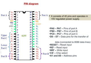
  • 11. •PA0 – PA7 – Pins of port A •PB0 – PB7 – Pins of port B •PC0 – PC7 – Pins of port C •D0 – D7 – Data pins for the transfer of data (connected to 8086 data lines) •RESET – Reset input •RD’ – Read input •WR’ – Write input •CS’ – Chip select •A1 and A0 – Address pins  It consists of 40 pins and operates in +5V regulated power supply. PIN diagram
  • 12. It consists of three 8-bit bidirectional I/O ports( 24 lines) through which the input, output devices are connected. 1. PORT A 2. PORT B 3. PORT C. Port C is further divided into two 4-bit ports i.e. port C lower and port C upper and port C I/O ports  Each port has unique address and data to read/write The pins A0, A1 will select the ports which is to be connected to the D0 to D7 CS’ – Chip select lines used to select the 8255, since multiple 8255 are connected When CS’ =0, that particular 8255 is selected Selection of port(commands to control blocks) When A0, A1=00, port A is selected =01 , port B is selected =10 , port C is selected =11, control register is selected for programming As soon as we connect 8255, we can program using control register
  • 14.  This unit accepts control signals ( RD’, WR’ ) and also inputs from address(A1, A0) bus and issues commands to control blocks .  It has the following pins. CS’ , RD’ , WR’ , RESET , A1 , A0 RESET : The 8255 is placed into its reset state if this input line is a logical 1  This is a tristate bidirectional buffer used to interface 8255 to microprocessor system data bus.  Data is transmitted or received by the buffer on execution of input or output instruction by the microprocessor. 1. Data bus buffer 2. Read/Write control logic  These block receive control from the microprocessor and issues commands to their respective ports.  2 groups of control blocks are present  Group A [Port-A (PA) & Port C Upper PCU(PC7 –PC4)] consist of port A and port C upper.  Group B [Port-B (PB )& Port C Lower PCL ( PC3 –PC0)] consists of port C lower and port B 3. Control block
  • 15. Modes of operation of 8255 1. Bit set/Reset (BSR) mode The BSR mode is used to set or reset the bits in port C. 2. I/O mode. The I/O mode is further divided into 3 modes: (i) mode 0 : all ports function as simple Input/output  Each of the port will work independently. Port A, Port B can be configured as simple 8 bit Input/output port without handshaking.  Two halves of Port C together work as 8 bit port or Port C as two 4-bit ports (ii) mode 1 I/O with handshake  Group A consist of port A (8 bit) and upper half of port C (4 bit) and Group B consist of port A (8 bit) and lower half of port C (4 bit)  port A and port B can be programmed as 8 bit input or output ports with 4 lines of port C in each group is used for handshaking (iii) mode 2 Bidirectional data transfer  Only port A can be used as bidirectional port.  Handshaking signals are provided on five lines of port C(PC3 –PC7) Two primary modes
  • 16. 8255 has 8 bit control register 8255 ports can be configured for operation by writing appropriate control word When A0, A1=11, control register is used for programming by setting the control word control register control word format For parallel I/O When D7=1, the word loaded into the control register is a mode definition word D7=0, it is taken as a bit set or reset word Appropriate words are set or reset depends on the type of operation desired, and loaded into the control register Control words defines the complete function of PPI. They are loaded before any transmission or reception
  • 17. For BSR mode S/R = 1 for set =0 for reset  Depending upon the value if CS’, A1 and A0 we can select different ports in different modes as input-output function or BSR.  This is done by writing a suitable word in control register (control word D0-D7).
  • 21. Basics of serial communication Transmitter: - A parallel-in, serial-out shift register Receiver: - A serial-in, parallel-out shift register. In parallel transmission, number of data lines depends on number of bits to be transmitted For long distance communication, parallel transmission is impractical(increase in cost)
  • 22. a) Simplex mode Data is transmitted only in one direction over a single communication channel. example, the processor may transmit data for a CRT display unit in this mode. b) Duplex Mode data may be transferred between two transreceivers in both directions simultaneously. c) Half Duplex mode  data transmission may take place in either direction, but at a time data may be transmitted only in one direction. A computer may communicate with a terminal in this mode. It is not possible to transmit data from the computer to the terminal and terminal to computer simultaneously. Basic Modes of serial data transmission a) Simplex b) Duplex c) Half Duplex
  • 23. Serial communication interface -8251 INTEL 8251 -USART - UNIVERSAL SYNCHRONOUS ASYNCHRONOUS RECEIVER TRANSMITTER (USART)  Programmable chip designed for synchronous and asynchronous serial data transmission  28 pin DIP  Coverts the parallel data into a serial stream of bits suitable for serial transmission.  Receives a serial stream of bits and convert it into parallel data bytes to be read by a microprocessor.
  • 25. Internal Block diagram of 8251 Internal architecture consists of Five Sections  Read/Write Control Logic  Transmitter Sections  Receiver Sections  Data Bus Buffer- 8 bit Bidirectional bus.  Modem Controller
  • 26. 1. Read/Write Control Logic  Interfaces the chip with MPU  Determine the functions according to the control word  Monitors data flow – Chip Select When this signal goes low, 8251 is selected by microprocessor unit(MPU) for communication – Control/Data When this signal is high, the control register or status register is addressed When it is low, the data buffer is addressed Control and Status register is differentiated by and signals, respectively – Write writes in the control register or sends outputs the data to the data buffer. This connected to IOW or MEMW – Read Either reads a status from status register or accepts data from the data buffer This is connected to either IOR or MEMR CLK - Clock Connected to system clock Necessary for communication with microprocessor. clock Frequency is 30 times greater than data rate of Tx.
  • 27. control Register-16 bit register Accessed as an output port when =1 status register- Checks the status of a peripheral RESET = 1, forces 8251 is in ideal mode.  It remain in the ideal mode until a new set of control word is written into 8251 to program its functions  (Control/Data) signal along with read() and write () signal inform 8251, the data on the data bus is either a data , control word or status information
  • 28.  Converts parallel data received from microprocessr unit(MPU) into serial data 2. Transmitter It consists of Transmitter buffer and transmit control It has two registers 1. Buffer Register : To hold eight bits of data 2. Output Register : Converts eight bits into a stream of serial bits Transmits data on TxD pin with appropriate framing bits(Start and Stop) TxD – Transmit Data Serial bits are transmitted on this line – Transmitter Clock Controls the rate at which bits are transmitted TxRDY – Transmitter Ready Can be used either to interrupt the MPU or indicate the status  It goes high when the USART is ready to accept data and its buffer register is empty TxEMPTY – Transmitter Empty Logic 1 on this line indicate that the output register is empty Signals in Transmitter Section
  • 29.  Receives serial bits from peripheral(I/O or memory)  Converts serial bits into parallel word(data)  Transfers the parallel word to the MPU 3. Receiver The section has two registers Input Register Buffer Register RxD – Receive Data Bits are received serially on this line and converted into parallel byte in the receiver input – Receiver Clock Controls the rate at which bits are transmitted RxRDY – Receiver Ready It goes high when the USART has a character in the buffer register and is ready to transfer it to the MPU Signals Associated with Receiver Section
  • 30. Used to establish data communication modems over telephone line Used to convert digital signals from these devices into analog signals that can be transmitted over telephone lines or cable networks. 4. Modem Controller - Data Set Ready Normally used to check modem condition if the Data Set is ready when communicating with a modem - – Data Terminal Ready This output signal is used to tell modem that Data Terminal is ready. – Request to send Data This output signal is asserted to begin transmission. the receiver is ready to receive a data byte from modem – Clear to Send A low on this input enables the 8251A to transmit serial data if the TxE bit in the command byte is set to a “one”. Signals Associated with Modem Control  This is a tristate bidirectional buffer used to interface 8251 to microprocessor system data bus.  Data is transmitted or received by the buffer on execution of input or output instruction by the microprocessor. 5. Data bus buffer
  • 31. Control words Control words defines the complete function of UASRT. They are loaded before any transmission or reception Control word is split into two 1. Mode instruction 2. Command instruction 1. Mode instruction Th
  • 32. 2. Command instruction  After the mode instruction, command instruction should be issued to the USART.  It controls the operation of the USART within the basic frame work established by the mode instruction
  • 33. Status Word n the data communication systems it is often necessary to examine the “status” of the transmitter and receiver. It is also necessary for CPU to know if any error has occurred during communication.
  • 34. (i) Asynchronous Mode (Transmission) –MPU to perpheral Two modes of operation 1. Synchronous mode 2. Asynchronous Mode modes of operation  MPU adds START bits prior to the serial data bits, followed by parity bit(optional) and STOP bits  This sequence is transmitted using TxD(transmit data) output pin to a peripheral when ( Transmitter clock- control the rate at which the data is transmitted) is low Asynchronous Mode (Receive) – perpheral to MPU  A low on RxD (Receive data) input line indicate a START bit .  Following the START bit, the data, STOP bits are received in input register  Then it is transferred to the buffer as parallel data  The RxRDY ( Receiver Ready) pin becomes high when the USART has a character in the buffer register and is ready to transfer it to the MPU
  • 35. (ii) Synchronous Mode (Transmission) –MPU to perpheral  The TxD output pin is high until the MPU sends character to USART  When (CTS)’(clear to send) line goes low, the first character(a SYNC character) is serially transmitted from UASRT during the falling edge of (TxC)’.  Data is shifted out at the same rate as (TxC)’ , over TxD output line  If the CPU buffer becomes empty, the SYNC character or characters are inserted in the data stream over TxD output. Synchronous Mode (Receiver)  synchronization can be achieved internally or externally. The data on RxD pin is sampled on rising edge of the RxC.  content of the receiver buffer is compared with the first SYNC character at every edge until it matches  When the characters match, the hunting stops.  The SYNDET pin set high and is reset automatically by a status read operation.
  • 37. A/D Interface - ADC 0808/0809  The analog to digital converter chips 0808 and 0809 are 8-bit CMOS, successive approximation converters. conversion time. - the time taken to produce a valid output binary code for an applied input voltage. When we refer to a converter as high speed, it has a short conversion time.
  • 38. Features  conversion delay is 100 µs at a clock frequency of 640 kHz  do not need any external zero or full scale adjustments  have a 3:8 analog multiplexer(at a time eight different analog inputs can be connected )  Out of these eight inputs only one can be selected for conversion by using address lines ADD A, ADD B and ADD C, PIN diagram
  • 39. operation  ADC has 8 input channels ,  3 bit address line (A, B, C) is used to select the desired input channel  The address must be latched for at least 50ns using Address latch enable (ALE) signal  After 2.5 s , the Start Of Conversion(SOC) signal must be send high then low to start conversion process.  End of conversion is indicated by End Of Conversion(EOC) signal  Microprocessor can read the digital word by enabling the output enable signal. Timing diagram
  • 40. Interfacing the ADC ADC is interfaced with 8086 through 8255 Programmable Peripheral Interface chip  PortA of 8255 chip is used as the input port. (Port B, Port C can be used)  PC7 pin of PortCupper is connected to the (EOC) Pin of the A/D converter.  The portClower is used as output port. (Port A, Port B can be used)  The PC0-PC2 lines are connected to three address pins(A, B,C) of 0808 to select input channels. The PC3 pin is connected to the Start of Conversion (SOC) pin and ALE pin of ADC 0808/0809.
  • 41. MVI A, 98H ; Set Port A and Cupper as input, CLower as output OUT 03H ; Write control word 8255-I to control Wordregister XRA A ; Clear the accumulator OUT 02H ; Send the content of Acc to Port Clower to select IN0 MVI A, 08H ; Load the accumulator with 08H OUT 02H ; ALE and SOC will be 0 XRA A ; Clear the accumulator OUT 02H ; ALE and SOC will be low. READ: IN 02H ; Read from EOC (PC7) RAL ; Rotate left to check C7 is 1. JNC READ ; If C7 is not 1, go to READ IN 00H ; Read digital output of ADC STA 8000H ; Save result at 8000H HLT ; Stop the program •Port A: Used to transfer the ADC's digital data output to the MPU •Port C: Used for control signals program
  • 42. D/A Interface - DAC 0800 D/A converter converts the digital signal into analog signal Several techniques are employed for digital to analog conversion. i. Weighted resistor network ii. R-2R ladder network iii. Current output D/A converter 1. Resolution: It is a change in analog output for one LSB change in digital input. the smallest increment of output that the DAC can produce for LSB change Resolution for n bit digital input is =(1/2n )*Vref. Vref = reference voltage eg. n=8 (i.e.8-bit DAC), Vref =5V’ then, resolution = 1/256*5V=39.06mV 2. Settling time: It is the time required for the DAC to settle from its initial output to steady state output(final value) Characteristics:
  • 43.  DAC require a reference analog voltage (Vref) or current (Iref) source.  DAC0800 is available as a 16-pin IC in DIP  DAC is an 8-bit, high speed, current output with settling time (conversion time) of 100 ns.  It produces complementary current output, which can be converted to voltage by using simple resistor load.  DAC require a positive and a negative supply voltage in the range of ± 5V to ±18V.  Resolution of the DAC is 39.06mV Features: PIN diagram
  • 44. Interfacing the DAC DAC is interfaced with 8086 through 8255 Programmable Peripheral Interface chip  PortA of 8255 chip is used as the input port. (Port B, Port C can be used)-Digital Input MVI A, DATA ; Load 8-bit data to be sent at the input of 0808 DAC OUT 00 ; Send data on port A. input words.
  • 45. Keyboard/Display Controller -INTEL 8279  8279 simultaneously drives the display of a system and interfaces a Keyboard with the microprocessor  8279 provides two interfaces: keyboard interface and Display interface  8279 has two modes of operation: Input(keyboard) mode and output(Display) mode 1. Keyboard interface  It scans the Keyboard to identify if any key has been pressed and sends the code of the pressed key to the microprocessor  8279 transmits the data received from the microprocessor, to the display device. 2. Display interface 8279 provides 1. A set of four scan lines and eight return lines for interfacing keyboards. 2. A set of eight output lines for interfacing display.
  • 46. PIN diagram •A0: Selects data (0) or control/status (1) for reads and writes between micro and 8279. •BD: Output that blanks the displays. •CLK: Used internally for timing. Max is 3 MHz. •CNTL/STB: Control/strobe, connected to the control key on the keyboard. •CS: Chip select that enables programming, reading th keyboard, etc. •DB7-DB0: Consists of bidirectional pins that connect to data bus on micro. •IRQ: Interrupt request, becomes 1 when a key is pressed, data is available. •OUT A3-A0/B3-B0: Outputs that sends data to the most significant/least significant nibble of display. •RD(WR): Connects to 8086's IORC or RD signal, reads data/status registers. •RESET: Connects to system RESET. •RL7-RL0: Return lines are inputs used to sense key depression in the keyboard matrix. •Shift: Shift connects to Shift key on keyboard. •SL3-SL0: Scan line outputs scan both the keyboard and displays.
  • 47. Internal Block diagram of 8279 1. Keyboard sections 2. Display session 3. Scan session 4. Microprocessor interface and control section 4 sessions
  • 48.  The 8 return lines (RL7 — RL0) are buffered and latched by the return buffers during each row scan in scanned keyboard or sensor matrix mode  In strobed input mode, the contents of the return lines are transferred to the FIFO RAM on the rising edge of the shift and control/strobe (CNTL/STB) line pulse. 1. Keyboard sections Return Buffers Keyboard Debounce and Control FIFO/Sensor RAM FIFO/Sensor RAM and Status Logic This section consists of Return Buffers: Keyboard Debounce and Control:  This section is enabled only during scanned key board mode  return lines are scanned, looking for key closures in that row.  If it detects a closed switch, the Keyboard debounce unit waits for 10 ms.  After the debounce period(10 ms), if the key continues to be detected, code of the Key is directly transferred to the FIFO sensor RAM along with SHIFT and CONTROL key status
  • 49. Two key depressions modes in keyboard section 2-key lockout N-key rollover. 2-key lockout mode If two keys are pressed simultaneously, only the first key is recognized. N-key rollover mode simultaneous keys are recognized and their codes are stored in FIFO.  . FIFO RAM status keeps track of the number of characters in the FIFO and whether it is full or empty.  Interrupt request (IRQ) signal is high when the FIFO is not empty, FIFO/Sensor RAM: This is a dual function 8 x 8 RAM. In scanned keyboard and strobed input modes, it is a FIFO. Each new entry is written into successive RAM positions and then read in order of entry. In sensor matrix mode, the memory is a sensor RAM. Each row of the sensor RAM is loaded with the status of the corresponding row of sensor in the sensor matrix FIFO/sensor RAM status:
  • 50. 2. Display section Display RAM Display register Display address register This section consists of Display RAM holds the 1.address of the byte currently being written or read by the microprocessor 2. scan count value.  The display section consists of 16 x 8 display RAM.  The microprocessor read from or write into any location of the display RAM.  In decoded mode, 8279 uses first four locations of display RAM.  In encoded mode, 8279 uses first eight locations for 8 digit display and all 16 locations for 16 digits display Display address register Display registers are two 4-bit registers A(A0-A3) and B(B0-B3). They hold the bit pattern of character to be displayed. The contents of display registers A and B can be blanked and inhibited individually. Display register
  • 51.  In decoded scan mode, the output of scan lines will be similar to a 2-to-4 decoder.  In encoded scan mode, the output of scan lines will be binary count, and so an external decoder should be used to convert the binary count to decoded output lines(SC3 — SC0).  The scan lines are common for keyboard and display. 3.Scan section scan counter has two modes Encoded mode and decoded mode. The scan section has a scan counter and four scan lines, SL0 to SL3. 4. Microprocessor unit(MPU) interface section  The MPU interface section takes care of data transfer between 8279 and the processor  consists of data buffers, I/O control, control and timing registers, and timing and control logic. Data Buffers 8-bit bi-directional data lines DB0 to DB7 for data transfer between 8279 and 8086.
  • 52. Control signal A0, , , are used for read/write operation in 8279. When A0 = 0, data is transferred A0 =1 command word or status word is transferred. , determine the direction of data flow through the data buffers. I/O control store the keyboard and display modes and other operating conditions programmed by the 8086 when A0 = 1 . Control and Timing Registers: The timing control consists of the basic timing counter chain. The first counter is divided by N prescaler that can be programmed to give an internal frequency of 100 kHz. Timing Control:
  • 53. Three input modes for keyboard interface  Scanned keyboard mode  Scanned sensor matrix mode  Strobed input mode 1. Keyboard interface mode Operating Modes of 8279 1. Keyboard interface (input) modes 2. Display(output) modes Scanned keyboard mode In this mode, matrix to be interfaced in two ways : Encoded scan and decoded scan  In the encoded scan, an 8 x 8 keyboard or in decoded scan , a 4 x 8 Keyboard can be interfaced.  The code of key pressed with SHIFT and CONTROL status is stored into the FIFO RAM.
  • 54. Two output modes for keyboard interface  Left Entry(typewriter type)  Right Entry(calculator type) 2. Display interface mode  Displays the characters from left to right  Address 0 in the RAM is the left-most display character and address 7 is the right most display character Left Entry mode Scanned sensor matrix mode In this mode, a sensor array can be interfaced with 8279 using either encoder or decoder scans. With encoder scan 8 x 8 sensor matrix or with decoder scan 4 x 8 sensor matrix can be interfaced. In this mode, if the control line goes low, the data on return lines, is stored in the FIFO RAM byte by byte. Strobed input mode Right Entry mode displays characters from right to left
  • 55. 8279 Commands: 1. Keyboard/Display Mode Set Command (000)  used to program operating modes of keyboard and display.  Three least significant bits decide the keyboard mode and next two bits decide the display mode Display Keyboard
  • 56. 2. Program Clock Command (001)  All timing and multiplexing signals are generated by an internal prescaler.  prescaler divides the external clock by a programmable integer value to generate internal frequency Bits PPPPP determine the value of this integer which ranges from 2 to 31. internal frequency - 100 kHz 3. Read FIFO/Sensor RAM Command (010): AAA - address of the sensor RAM AI(autoincrement flag) =1, each successive read will be from the subsequent row of the sensor RAM To read data from FIFO/sensor RAM
  • 57. 4. Read Display RAM Command (011) To read data from display RAM AI(autoincrement flag) =1, display RAM address is incremented after each read comman AAAA) -address ‘of the 16 byte display RAM 5. Write Display RAM Command AI(autoincrement flag) =1, display RAM address is incremented after each write command to display RAM. AAAA) -address ‘of the 16 byte display RAM
  • 58. 6. Display Write Inhibit/Blanking Command (101)  display RAM data is sent on the two 4-bit ports (B3 — B0 and A3 —A0)  This two 4-bit pots can be individually inhibited or blanked with display write inhibit/blanking(BD) command. IW bits - mask nibble A (4-bit port A) and nibble B (4-bit port B) in applications requiring separate 4-bit display ports. BL bits -blank the individual nibbles. loads the blank code (All zeros, 20H, or All ones) 7. Clear Command (110): clear all the rows of the display RAM with a selectable blanking code, to clear status of FIFO RAM and to reset interrupt output line CD bits (CD0 — CD1 ) are used to select the blanking code
  • 59. Bit CD2, - set to 1, to clear display Bit CF, - set to 1 to clears the status of the FIFO, resets the interrupt output line and sets the sensor RAM address to 000. CA, - clear all bit, (combined effect of CD and CF); clears FIFO status. It also resynchronizes the internal timing chain. 8. End Interrupt/Error Mode Set Command (111): In sensor matrix mode,  if any change in sensor value is detected, IRQ line goes high at the end of a sensor matrix scan.  If the autoincrement flag = 0, IRQ line is cleared.  if autoincrement flag =1, End Interrupt Command clear the IRQ line. N key rollover mode, E bit =‘1’, the 8279 will operate in the Special Error Mode.
  • 60. Interrupt controller-8259 8086 has only two interrupt inputs, NMI and INTR.  If NMI is for a power failure interrupt, then only one interrupt for all the other applications.  So external priority interrupt controller is used to handle the interrupts  The Intel 8259A Programmable Interrupt Controller handles up to eight vectored priority interrupts for the microprocessor  It is cascaded to handle 64 vectored priority interrupts without additional circuitry.  It is packaged in a 28-pin DIP, uses NMOS technology, requiring no clock input.
  • 61. PIN diagram D0-D7 Bi-directional data lines. read control write control A0 Address line, to select control register chip select CAS0- CAS2 Bi-directional, 3 bit cascade lines. / Slave program / enable. INT Interrupt line, connected to INTR of microprocessor Interrupt ack, received active low from microprocessor IR0-IR7 Asynchronous IRQ input lines, generated by peripherals
  • 63. IRR stores all the interrupt request to serve them one by one on the priority basis. Interrupt Request Register (IRR): In-Service Register (ISR): This stores all the interrupt requests those are being served Priority resolver  Determines the priorities of the bits set in the IRR. IR0 has highest priority IR7 has lowest priority  The highest priority is selected and strobed into the corresponding bit of the ISR during INTA pulse Interrupt mask register (IMR) stores the bits required to mask the interrupt inputs based on priority resolver Interrupt Control Logic  This block manages the interrupt(INT) and interrupt acknowledge(INTA) signals sent to the microprocessor for serving one of the eight interrupt requests, and release vector address on to the data bus.
  • 64.  This tristate bidirectional buffer interfaces internal 8259A bus to the microprocessor system data bus.  Control words, status and vector information pass through data buffer during read or write operations. Data Bus Buffer  This block generates control signals necessary for cascade operations(more than one 8259)  Also generate buffer enable signals  8259A can be set up as a master (SP)’/(EN)’ =1) or slave (SP)’/(EN)’ =0) by slave program(SP)’/Enable buffer(EN)’ signal.  For a master the CASO-CAS2 pins are output pins and for slave these pins are inputs pins  In Master mode , 8259 sends the ID of the interrupting slave device on these lines.  The slave thus selected, will send its preprogrammed vector address on the data bus during the next INTA pulse. Read/Write Control Logic Read(RD) and Write(WR) inputs control the data flow on the databus when 8259 is selected by chip select(CP) input. Cascade Buffer/Comparator
  • 65. 1. One or more of the INTERRUPT REQUEST lines (IR7 -IR0) are high, corresponding IRR bit(s) is set. 2. 8259A sends an INT to the 8086 and 8086 responds in INTA pulse. 3. Then, the highest priority ISR bit is set, and the corresponding IRR bit is reset. Also release a CALL instruction onto the 8-bit Data Bus (D0 –D7) pins. 4. CALL instruction will initiate two more INTA pulses from 8086 to release the preprogrammed subroutine address onto the Data Bus. Interrupt sequence
  • 66. Traffic lights, which may also be known as stoplights, traffic lamps, traffic signals, signal lights, robots or semaphore, are signaling devices positioned at road intersections, pedestrian crossings and other locations to control competing flows of traffic. Traffic light controller INTERFACING TRAFFIC LIGHT WITH 8086  The Traffic light controller section consists of 12 Nos. point led’s arranged by 4Lanes in Traffic light interface card.  Each lane has Go(Green), Listen(Yellow) and Stop(Red) LED is being placed.
  • 68. Hardware Port A- control lights on N-S road Port B- control lights on W-E road Interfacing diagram to control 12 electric bulbs.  electric bulbs are controlled by relays  8255 control the relays by driver circuit  Driver circuit consists of 12 transistors. Actual PIN connection
  • 69. Find the port address
  • 73. LED DISPLAY interfacing  Light Emitting Diodes (LED) is the most commonly used components, usually for displaying digital states.  Typical uses of LEDs include alarm devices, timers and confirmation of user input such as a mouse click or keystroke. INTERFACING LED  Anode is connected through a resistor to GND & the Cathode is connected to the Microprocessor pin.  So when the Port Pin is HIGH the LED is OFF & when the Port Pin is LOW the LED is turned ON.
  • 77. LCD display.  LCD modules are available which have built-in drivers for LCD and interfacing circuitry to interface them to microprocessor/microcontroller systems.  These LCD modules allow display of characters as well as numbers.  They are available in 16 x 2, 20 × 1, 20 × 2, 20 × 4 and 40 × 2 sizes.  The main advantage of using LCD is modules is that they require very less power. In this module the display is organized as two lines, each of 20 characters. The module has 14-pins. The voltage at VEE pin is adjusted by a potentiometer to adjust the contrast of the of the LCD. LCD Interfacing:
  • 81. 1.Initialize the 8255 PPI: •Set up the 8255 PPI ports for LCD communication. Port A is used to send data/commands to the LCD, and Port C is used for control signals(RS,R/W and E). •Control Word (80H): Configures Port A and Port C for output. 2. Initialize the LCD: •Send the initialization commands to the LCD: •Set 8-bit mode, 2-line display, and 5x7 character matrix. •Turn on the display, enable the cursor. •Set the entry mode to increment the cursor position after each character. •Clear the display. Procedure for the Code: 3.Display a String: •Load the starting address of the string(1200H)into the source index register(SI). •Use a loop to read each character from memory and send it to the LCD. •After writing a character, move to the next character and repeat until the entire string is displayed.
  • 82. 7.Repeat the Process: •After displaying the string, the program jumps back to START and repeats the process indefinitely. 4. CMDWT Subroutine: •Used to send commands to the LCD by writing to the control port (Port C of 8255), setting the RS and E pin accordingly. 5. DATWT Subroutine: •Used to send data (characters) to the LCD by writing to the data port (Port A of 8255) and setting the control signals to indicate data transfer. 6. Delay Subroutine: •Used to introduce a delay between consecutive commands and data writes to ensure the LCD has enough time to process each operation.