


Architecture and Programmingpart1_Microcontroller
- 1. 18EC 18 18ECC203J : Module 4 College of Engineering and Technology, SRM Institute of Science and Technology. Module 4: Intel 8051 – Architecture and Programming 2022 1
- 2. Overview Introduction Difference of 8086 Vs 8051 Family & Features of 8051 Architecture, Pin Description of the 8051 Register set Memory & IO addressing Interrupts & Stack in the 8051 Applications 2022 2
- 3. ■ Its not an exaggeration if I say that, today there is no electronic gadget on the earth which is designed without a Microcontroller. Ex: communication devices, digital entertainment, portable devices etc… Not believable ??? See the next slide Why do we need to learn Microcontrollers ? 2022 3
- 4. ■ Personal information products: Cell phone, pager, watch, pocket recorder, calculator ■ Laptop components:mouse, keyboard, modem, fax card, sound card, battery charger ■ Home appliances:door lock, alarm clock, thermostat, air conditioner, TV remote, VCR, small refrigerator, exercise equipment, washer/dryer, microwave oven ■ Industrial equipment: Temperature/pressure controllers, Counters, timers, RPM Controllers ■ Toys: video games, cars, dolls, etc. 2022 4
- 5. So, A good designer should always know what type of controller he/she is using ,their architecture, advantages , disadvantages, ways to reduce production costs and product reliability etc…. O.K ???? 2022 5
- 6. Then What is a Microcontroller ? CPU RAM ROM I/O Port Timer Serial COM Port ■ A smaller computer ■ On-chip RAM, ROM, I/O ports... ■ Example : Motorola’s 6811, Intel’s 8051, Zilog’s Z8 and PIC 16X A single chip Microcontroller 2022 6
- 7. How is it different from a Microprocessor ?? ■ General-purpose microprocessor CPU for Computers No RAM, ROM, I/O on CPU chip itself Example : Intel’s x86, Motorola’s 680x0 CPU General- Purpose Micro- processor RAM ROM I/O Port Timer Serial COM Port Data Bus Address Bus 2022 7
- 8. Microprocessor ■ CPU is stand-alone, RAM, ROM, I/O, timer are separate ■ ■ ■ ■ designer can decide on the amount of ROM, RAM and I/ O ports. expansive versatility general-purpose Microcontroller • CPU, RAM, ROM, I/O and timer are all on a single chip • fix amount of on-chip ROM, RAM, I/O ports • Highly bit addressable • for applications in which cost, power and space are critical • single-purpose Microprocessor vs. Microcontroller 2022 8
- 9. EVOLUTION Flashback !!!! In the year 1976, Motorola created a Microprocessor chip called 6801 which replaced its brother 6800 with certain add-on chips to make a computer. This paved the way for the new revolution in the history of chip design and gave birth to a new entity called MICROCONTROLLER. The INTEL bagged the credit of producing the first Microcontroller8048 with a CPU and 1K bytes of EPROM, 64 Bytes of RAM an 8-Bit Timer and 27 I/O pins in 1976. 2022 9
- 10. Evolution contd… ■ Then followed the most popular controller 8051 in the year 1980 with 4K bytes of ROM, 128 Bytes of RAM , a serial port, two 16-bit Timers , and 32 I/O pins. ■ The 8051 family has many additions and improvements over the years and remains a most soughtafter tool for todays circuit designers. ■ The same INTEL introduced a 16 bit controller 8096 in the year 1982 2022 10
- 11. ■ Later INTEL introduced 80c196 series of 16-bit microcontrollers for mainly industrial applications ■ Microchip, another company has introduced a microcontroller PIC 16C64 an 8-bit in the year 1985. ■ 32-bit microcontrollers have been developed by IBM and Motorola-MPC 505 is a 32-bit RISC controller of Motorola ■ The 403 GA is a 32 -bit RISC embedded controller of IBM 2022 11
- 12. ARM Controllers ■ In recent times ARM company (Advanced Risc machines) has developed and introduced 32 bit controllers which are highend application devices, especially communication devices like mobiles , ipods etc..(Refer www.arm.com) 2022 12
- 13. 2022 13 INTEL FAMILY OF MICROCONTROLLERS, FEATURE OF 8051 MICROCONTROLLER
- 15. Microcontrollers from different manufacturers •Atmel •ARM •Intel •8-bit •8XC42 •MCS48 •MCS51 •8xC251 •16-bit •MCS96 •MXS296 •National Semiconductor •COP8 •Microchip •12-bit instruction PIC •14-bit instruction PIC •PIC16F84 •16-bit instruction PIC •NEC •Motorola •8-bit •68HC05 •68HC08 •68HC11 •16-bit •68HC12 •68HC16 •32-bit •683xx •Texas Instruments •TMS370 •MSP430 •Zilog •Z8 •Z86E02 2022 15
- 16. MCS-51 “Family” of Microcontollers Feature ROM 8031 8051 8052 8751 NO 4kB 8kB 4kB UV Eprom RAM (Bytes) 128 128 256 128 TIMERS 2 2 3 2 I/O PINS 32 32 32 32 SERIAL PORTS 1 1 1 1 6 6 8 6 INTERRUPT SOURCES 2022 16
- 17. Microcontroller Architectures CPU Program + Data Data Bus Von Neumann Architecture CPU Program Address Bus Data Bus Harvard Architecture Memory Data Address Bus Fetch Bus Memory Address Bus 0 0 0 2 n 2022 17
- 18. 2022 18 Von-Neumann Architecture Harvard Architecture Single memory to be shared by both code and data. Separate memories for code and data. Processor needs to fetch code in a separate clock cycle and data in another clock cycle. So it requires two clock cycles. Single clock cycle is sufficient, as separate buses are used to access code and data. Higher speed, thus less time consuming. Slower in speed, thus more time-consuming. Simple in design. Complex in design.
- 19. Important Features of 8051 ■ 4K bytes ROM ■ 128 bytes RAM ■ Four 8-bit I/O ports ■ Two 16-bit timers ■ Serial interface ■ 64K external code memory space ■ 64K data memory space 2022 19
- 20. 2022 20 Architecture of 8051, Pin descriptions of 8051, Register Sets, Operational features of 8051.
- 21. Pin Description of the 8051 ■ The 8051 is a 40 pin device, but out of these 40 pins, 32 are used for I/O. ■ 24 of these are dual purpose, i.e. they can operate as I/O or a control line or as part of address or date bus. 2022 21
- 22. PORTS OF 8051 ■ 8051 has 4 Ports. Port 0, Port1, Port2 , Port3 ■ Port 0 is a dual purpose port, it is located from pin 32 to pin 39 (8 pins). To use this port as both input/output ports each pin must be connected externally to a 10 k ohm pull-up resistor.This is because Port 0 is an open drain. Simple ex: BACK MOV A, #22 MOV P0 ,A ACALL DELAY CPL A SJMP BACK 2022 22
- 23. Port 0 with Pull-Up Resistors 2022 23
- 24. ■ Port 1 is a dedicated I/O port from pin 1 to pin 8.Upon reset it is configured as outport. It is generally used for interfacing to external device thus if you need to connect to switches or LEDs, you could make use of these 8 pins,but it doesn’t need any pull-up resistors as it is having internally. ■ Port 2 is like a P0 and it is a dual-purpose port.(Pins 21 through 28) It can be used for general I/O or as the high byte of the address bus for designs with external code memory.Like P1 ,Port2 also doesn’t require any pull-up resistors Ports…. 2022 24
- 25. Ports contd… ■ Port 3 is also dual purpose but designers generally avoid using this port unnecessarily for I/O because the pins have alternate functions which are related to special features of the 8051. Indiscriminate use of these pins may interfere with the normal operation of the 8051. The pin numbers are from 10 to 17. The other functions are below. Pin10 – RXD, Pin11 – TXD, Pin12 – INT0 complement Pin13 – INT1, Pin14 – T0, Pin15 – T1, Pin16 – WR Pin17 – RD complement. ■ However, for a programmer, it is the same to program P0, P1, P2 and P3. ■ All the ports upon RESET are configured as output. To use any 2022 25
- 26. Alternate functions of P3 2022 26
- 27. 2022 27 Additionally, the other pins are as follows : •Pin20 – GND (Ground) •Pin40 – VCC (Supply) •Pin9 – RST (Reset) •Pin18 – XTAL1 (Oscillator) •Pin19 – XTAL2 (Oscillator) •Pin29 – PSEN (Program Store Enable) •Pin30 – ALE (Address Latch Enable) •Pin31 – EA (External Access)
- 28. Block diagram of 8051 2022 28
- 29. 2022 29
- 30. 2022 30 Functional Description Block : Accumulator - SFR - It can be accessed through its SFR adder 0E0H. B Register - Use as temporary register . - store upper byte Result of MUL & DIV. - access through SFR adder 0F0H. Stack Pointer - Define anywhere on chip 128 byte RAM. - It is Initialised to 07H address (after rest) . - Data Pointer - - 16 bit register - -Access external memory up to 64KB.
- 31. 2022 31 Functional Description Block Program Status Word - Reflect status ALU performing operation. Port 0 to 3 - Each latch and corresponding drivers of port 0 to 3 is allotted to the corresponding on chip I/O port. Serial Data Buffer - Two Independent Register : TX Buffer (8bit) & RX Buffer(8bit). Program Counter - 16 bit wide - - Point to address of next instruction to be executed
- 32. 2022 32 Functional Description Block Timing & Control Unit - Deriver signal required for Internal operation of circuit . - Control signal required for controlling External System Bus. Oscillator - Generate basic timing control signal for operation of circuit using crystal oscillator. - ALU - - Perform 8 bit operation. - - Through TMP1 and TMP2 (each 8 bit). - Not access by User. SFR Register Bank - lie in range of 80H to 0FFH . - It can addressed using their respective address .
- 33. 2022 33 1. Oscillator and clock generator: All operations in a microcontroller are synchronized by the help of an oscillator clock. The oscillator clock generates the clock pulses by which all internal operations are synchronized. A resonant network connected through pins XTAL1 and XTAL2 forms up an oscillator. For this purpose a quartz crystal and capacitors are employed. The crystal run at specified maximum and minimum frequencies typically at 1 MHz to 16 MHz. 2. ALU: It is 8 bit unit. It performs arithmetic operation as addition, subtraction, multiplication, division, increment and decrement. It performs logical operations like AND, OR and EX-OR. It manipulates 8 bit and 16 bit data. It calculates address of jump locations in relative branch instruction. It performs compare, rotate and compliment operations.
- 34. 2022 34 a. Accumulator(A-reg): It is 8 bit register. Its address is E0H and it is bit and byte accessible. Result of arithmetic & logic operations performed by ALU is accumulated by this register. Therefore it is called accumulator register. It is used to store 8 bit data and to hold one of operand of ALU units during arithmetical and logical operations. b. B-register: It is special 8 bit math register. It is bit and byte accessible. It is used in conjunction with A register as I/P operand for ALU. It is used as general purpose register to store 8 bit data. c. PSW: It is 8 bit register. Its address is D0H and It is bit and byte accessible. The format of flag register is as shown below:
- 35. 2022 35 c. PSW: It is 8 bit register. Its address is D0H and It is bit and byte accessible. It has 4 conditional flags or math flags which sets or resets according to condition of result. It has 3 control flags, by setting or resetting bit required operation or function can be achieved. The format of flag register is as shown below: d. FLAG: 1. Carry Flag(CY): During addition and subtraction any carry or borrow is generated then carry flag is set otherwise carry flag resets. It is used in arithmetic, logical, jump, rotate and Boolean operations. 2. Auxiliary carry flag(AC): If during addition and subtraction any carry or borrow is generated from lower 4 bit to higher 4 bit then AC sets else it resets. It is used in BCD arithmetic operations. 3. Overflow flag(OV): If in signed arithmetic operations result exceeds more than 7 bit than OV flag sets else resets. It is used in signed arithmetic operations only. 4. Parity flag(P): If in result, even no. of ones "1" are present than it is called even parity and parity flag sets. In result odd no. of ones "1"are present than it is called odd parity and parity flag resets.
- 36. 2022 36 ii. CONTROL FLAGS: 1. FO: It is user defined flag. The user defines the function of this flag. The user can set ,test n clear this flag through software. 2. RS1 and RS0: These flags are used to select bank of register by resetting those flags which are as shown in table : 3. Program counter (PC): The Program Counter (PC) is a 2-byte address which tells the 8051 where the next instruction to execute is found in memory. It is used to hold 16 bit address of internal RAM, external RAM or external ROM locations. 4. Data pointer register (DTPR): It is a 16 bit register used to hold address of external or internal RAM where data is stored or result is to be stored. It is used to store 16 bit data. It is divided into2- 8bit registers, DPH-data pointer higher order (83H) and DPL-data pointer lower order (82H). 5. Stack pointer (SP): It is 8-bit register. It is byte addressable. Its address is 81H. It is used to hold the internal RAM memory location addresses which are used as stack memory.
- 37. 2022 37 iii. Special function Registers(SFR): The 8051 microcontroller has 11 SFR divided in 4 groups: A. Timer/Counter register: 8051 microcontroller has 2-16 bit Timer/counter registers called Timer-reg-T0 And Timer/counter Reg-T1.Each register is 16 bit register divide into lower and higher byte register as shown below: These register are used to hold initial no. of count. All of the 4 register are byte addressable. 1. Timer control register: 8051 microcontroller has two 8-bit timer control register i.e. TMOD and TCON register. TMOD Register: it is 8-bit register. Its address is 89H. It is byte addressable. It used to select mode and control operation of time by writing control word. 2. TCON register: It is 8-bit register. Its address is 88H. It is byte addressable. Its MSB 4- bit are used to control operation of timer/ counter and LSB 4-bit are used for external interrupt control.
- 38. 2022 38 B. Serial data register: 8051 micro controller has 2 serial data register viz. SBUF and SCON. 1. Serial buffer register (SBUF): it is 8-bit register. It is byte addressable .Its address is 99H. It is used to hold data which is to be transferred serially. 2. Serial control register (SCON): it is 8-bit register. It is bit/byte addressable. Its address is 98H. The 8-bit loaded into this register controls the operation of serial communication. C. Interrupt register: 8051 µC has 2 8-bit interrupt register. 1. Interrupt enable register (IE): it is 8-bit register. It is bit/byte addressable. Its address is A8H.it is used to enable and disable function of interrupt. 2. Interrupt priority register (IP): It is 8-bit register. It is bit/byte addressable. Its address is B8H. it is used to select low or high level priority of each individual interrupts. D. Power control register (PCON): it is 8-bit register. It is byte addressable .Its address is 87H. Its bits are used to control mode of power saving circuit, either idle or power down mode and also one bit is used to modify baud rate of serial communication.
- 39. Special Function Registers DATA registers CONTROL registers •Timers •Serial ports •Interrupt system •Analog to Digital converter •Digital to Analog converter etc.. Addresses 80h – FFh Direct Addressing is used to access SFRs 2022 39
- 40. List of Registers (*Denotes the SFRs) 2022 40
- 41. Contd… 2022 41
- 43. 2022 43 Features of 8051 Microcontroller An 8051 microcontroller comes bundled with the following features − •4KB bytes on-chip program memory (ROM) •128 bytes on-chip data memory (RAM) •Four register banks •128 user defined software flags •8-bit bidirectional data bus •16-bit unidirectional address bus •32 general purpose registers each of 8-bit •16 bit Timers (usually 2, but may have more or less) •Three internal and two external Interrupts •Four 8-bit ports,(short model have two 8-bit ports) •16-bit program counter and data pointer •8051 may also have a number of special features such as UARTs, ADC, Op-amp, etc.
- 44. 2022 44 Memory and I/O addressing by 8051 Interrupts and Stack of 8051
- 45. Program Memory Stores program to be executed Implemented by EPROM Further divided into on chip (internal )- 4KB and external- 64 KB Data Memor y Stores intermediate results, variables, consta nts Implemented by RAM INTERNAL-128 bytes of RAM +SFR EXTERNAL – 64 KB Memory Addressing 2022 45
- 46. 2022 46 • ROM ( READ ONLYMEMORY ) • 8051 can address 4K bytes on chip memory – map range 0000 TO 0FFFh • IT can address 64 KB external memory map range – 0000 TO FFFFh • Memory map of internal and external program overlaps • The internal and external ROM distinguished by PSEN’ signal • ROM less version of 8051 – PSEN’ used to access external memory PROGRAM ME M ORY - ROM
- 47. 2022 47 ROM - program
- 48. 2022 48 • EXTERNAL RAM • 8051 supports 64KB external data memory- range – 0000 to FFFFh • Accessed by DPTR • 8051 generates RD’, WR’ during external access . • CS’ can be derived from address lines D A T A M E M O R Y - RAM
- 49. 2022 49 ON C H I P ( I N T E R N A L ) RAM ONCHI P RAM SF R RANG E: 80h TO FFh Direct Addressi ng only Direct & Indirect addressi ng RANGE : 00h TO 7Fh • 128 BYTES RAM BLOC K
- 50. 2022 50 RA M
- 51. RAM memory space allocation in the 8051 7FH 30H 2FH 20H 1FH 18H 17H 10H 0FH 08H 07H 00H Register Bank 0 Stack) Register Bank 1) Register Bank 2 Register Bank 3 Bit-Addressable RAM Scratch pad RAM 2022 51
- 53. 2022 53 Registers 08 07 06 05 04 03 02 01 00 R7 R6 R5 R4 R3 R2 R1 R0 10 0F 1F 18 17 Bank 3 Bank 2 Bank 1 Bank 0 Four Register Banks Each bank has R0-R7 Selectable by psw.2,3
- 54. 2022 54 Bit Addressable Memory 20h – 2Fh (16 locations X 8-bits = 128 bits) 7F 78 1A 10 0F 08 07 06 05 04 03 02 01 00 2F 2E 2D 2C 2B 2A 29 28 27 26 25 24 23 22 21 20 Bit addressing: mov C, 1Ah or mov C, 23h.2
- 55. 2022 55 Special Function Registers ❑ DATA registers ❑ CONTROL registers ❖ Timers ❖ Serial ports ❖ Interrupt system ❖ Analog to Digital converter ❖ Digital to Analog converter ❖ Etc. Addresses 80h – FFh Direct Addressing used to access SPRs
- 56. 2022 56 8051 microcontrollers have 4 I/O ports each of 8-bit, which can be configured as input or output. Hence, total 32 input/output pins allow the microcontroller to be connected with the peripheral devices. •Pin configuration, i.e. the pin can be configured as 1 for input and 0 for output as per the logic state. • Input/Output (I/O) pin − All the circuits within the microcontroller must be connected to one of its pins except P0 port because it does not have pull-up resistors built-in. • Input pin − Logic 1 is applied to a bit of the P register. The output FE transistor is turned off and the other pin remains connected to the power supply voltage over a pull-up resistor of high resistance. I/O ADDRESSING
- 57. 2022 57 •Port 0 − The P0 (zero) port is characterized by two functions − • When the external memory is used then the lower address byte (addresses A0A7) is applied on it, else all bits of this port are configured as input/output. • When P0 port is configured as an output then other ports consisting of pins with built-in pull-up resistor connected by its end to 5V power supply, the pins of this port have this resistor left out. Input Configuration If any pin of this port is configured as an input, then it acts as if it “floats”, i.e. the input has unlimited input resistance and in-determined potential. Output Configuration When the pin is configured as an output, then it acts as an “open drain”. By applying logic 0 to a port bit, the appropriate pin will be connected to ground (0V), and applying logic 1, the external output will keep on “floating”. In order to apply logic 1 (5V) on this output pin, it is necessary to build an external pullup resistor.
- 58. 2022 58 Interrupts are the events that temporarily suspend the main program, pass the control to the external sources and execute their task. It then passes the control to the main program where it had left off. 8051 has 5 interrupt signals, i.e. INT0, TFO, INT1, TF1, RI/TI. Each interrupt can be enabled or disabled by setting bits of the IE register and the whole interrupt system can be disabled by clearing the EA bit of the same register. IE (Interrupt Enable) Register This register is responsible for enabling and disabling the interrupt. EA register is set to one for enabling interrupts and set to 0 for disabling the interrupts. Its bit sequence and their meanings are shown in the following figure. Microcontrollers - 8051 Interrupts
- 59. 2022 59 EA IE. 7 It disables all interrupts. When EA = 0 no interrupt will be acknowledged and EA = 1 enables the interrupt individually. - IE. 6 Reserved for future use. - IE. 5 Reserved for future use. ES IE. 4 Enables/disables serial port interrupt. ET 1 IE. 3 Enables/disables timer1 overflow interrupt. EX 1 IE. 2 Enables/disables external interrupt1. ET 0 IE. 1 Enables/disables timer0 overflow interrupt. EX 0 IE. 0 Enables/disables external interrupt0. IP (Interrupt Priority) Register We can change the priority levels of the interrupts by changing the corresponding bit in the Interrupt Priority (IP) register as shown in the following figure. •A low priority interrupt can only be interrupted by the high priority interrupt, but not interrupted by another low priority interrupt.
- 60. 2022 60 •If two interrupts of different priority levels are received simultaneously, the request of higher priority level is served. •If the requests of the same priority levels are received simultaneously, then the internal polling sequence determines which request is to be serviced. - IP. 6 Reserved for future use. - IP. 5 Reserved for future use. PS IP. 4 It defines the serial port interrupt priority level. PT 1 IP. 3 It defines the timer interrupt of 1 priority. PX 1 IP. 2 It defines the external interrupt priority level. PT 0 IP. 1 It defines the timer0 interrupt priority level. PX 0 IP. 0 It defines the external interrupt of 0 priority level. TCON Register TCON register specifies the type of external interrupt to the microcontroller.
- 61. 2022 61 The register used to access the stack is called SP (stack pointer) register. The stack pointer in the 8051 is only 8 bits wide, which means that it can take value 00 to FFH. When 8051 powered up, the SP register contains value 07. Stack in the 8051
- 66. 2022 66
- 67. 2022 67
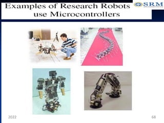
- 68. 2022 68
- 69. 2022 69
- 70. 2022 70