


![software development tools and true parallel implementation. Field Programmable Gate Array (FPGA)
are a family of programmable device based on an array of configurable logic blocks (CLBs), which gives
a great flexibility in prototyping, designing and development of complex hardware real time systems. The
structure of a FPGA can be described as an "array of blocks" connected together via programmable
interconnections. The main advantage of FPGA is the flexibility that they afford [ 3]. Xilinx Inc.
introduced the world's first FPGA, the XC2064 in 1985. The XC2064 contained approximately 1000
logic gate. Since then, the gate density of Xilinx FPGAs has increased thousands times. Recently there is
a lot of interest in the FPGA realization of neural networks which is reported by many researchers.
Mathematical model of an artificial neuron:
Mathematical model of artificial neuron
Where j p is the input value and w j is the corresponding weight value, A is the output of the neuron, and f
is a nonlinear activation function. Typically the activation function is chosen by the designer for specific
training algorithm , and then the weights will be adjusted by some learning rule so that the neuron input /
output relationship meet some specific goal.
Haitham Kareem Ali and Esraa Zeki Mohammed “Design Artificial Neural Network Using FPGA”
In layered neural networks, the neurons are organized in the form of layers. The neurons in a layer get
inputs from the previous layer and feed their output to the next layer. These type of networks are called
feed forward networks. Output connections from a neuron to the same or previous layer neurons are not
permitted. The input layer is made of special input neurons, transmitting only the applied external input to
their outputs. The last layer is called the output layer, and the layers other than input & output layers are
called the hidden layers. In a network, if there are input and output layers only, then it is called a single
layer network. Networks with one or more hidden layers are called multilayer networks.](https://image.slidesharecdn.com/fpgaimplementationofmultilayerfeedforwardneuralnetworkarchitectureusingvhdl-180710130354/85/Fpga-implementation-of-multilayer-feed-forward-neural-network-architecture-using-vhdl-5-320.jpg)

![One of the most important parts of a neuron is its activation function. The nonlinearity of the activation
function makes it possible to approximate any function.. This holds true for the nonlinear activation
function used at the output of neurons. A common activation function is the sigmoid function
Y = 1/1+ex
Efficient implementation of the sigmoid function on an FPGA is a difficult challenge faced by designers.
It is not suitable for direct implementation because it consists of an infinite exponential series. In most
cases computationally simplified alternatives of sigmoid function are used.
J. Renteria-Cedano, C. Perez-Wences, L. M. Aguilar-Lobo, J. R. Loo-Yau, J. A. Reynoso-
Hernandez “A Novel Configurable FPGA Architecture for Hardware Implementation of
Multilayer Feed forward Neural Networks Suitable for Digital Pre-Distortion Technique”
In this paper was presented a novel configurable architecture that allows implement any Multilayer Feed
forward Neural Network (MFNN) in a FPGA. The number of layers, number of neurons and threshold
function of a MFNN are configured sending specific codes to the FPGA. The logical resources of the
FPGA are optimized by taking into account the nature of the MFNN, this allows the programming only a
single neuron to perform all the inherent mathematical operations of a MFNN. This fact represents a
breakthrough for future development of DPD techniques based on artificial neural network.
A typical MFNN is divided in several sections or layers, basically the first and the last layer are referred
to the input and output layers, respectively, and the intermediate layers are known as hidden layers. Each
layer contains a set of interconnected units called neurons in which its output depends on its input and the
computational function.
Aydogan Savran, Serkan unsal “Hardware implementation of a Feed forward neural network
using FPGAs”
Accuracy has a great impact in the learning phase; so the precision of the numbers must be as high as
possible during training. However during the propagation phase, lower precisions are acceptable. The
resulting errors will be small enough to be neglected especially in classification applications. In the XOR
problem we applied, the input space is between –1 and 1. The training resulted in weights residing
between –2 and 2. We chose 8-bit precision for the system to cover the [-2,2] range, resulting in a](https://image.slidesharecdn.com/fpgaimplementationofmultilayerfeedforwardneuralnetworkarchitectureusingvhdl-180710130354/85/Fpga-implementation-of-multilayer-feed-forward-neural-network-architecture-using-vhdl-7-320.jpg)


![ART Structure
Cascade Correlation
The Cascade Correlation network was developed in 1990 by Scott E. Fahlman and Christian Lebiere [13].
It is an example of a growing network structure. Usually it is difficult to find a suitable network structure
for a given problem. In the majority of cases try-and-error is used, possibly supported by heuristic
methods. In Cascade Correlation networks the structure is part of the training process.
FIELD PROGRAMMABLE GATE ARRAYS
FPGA provide the next generation in the programmable logic devices. The word Field in the name refers
to the ability of the gate arrays to be programmed for a specific function by the user instead of by the
manufacturer of the device. The word Array is used to indicate a series of columns and rows of gates that
can be programmed by the end user. As compared to standard gate arrays, the field programmable gate
arrays are larger devices. The basic cell structure for FPGA is somewhat complicated than the basic cell
structure of standard gate array. The programmable logic blocks of FPGA are called Configurable Logic
Block (CLB).](https://image.slidesharecdn.com/fpgaimplementationofmultilayerfeedforwardneuralnetworkarchitectureusingvhdl-180710130354/85/Fpga-implementation-of-multilayer-feed-forward-neural-network-architecture-using-vhdl-17-320.jpg)


![Classification of FPGAs on user programmable switch technology is given in Fig below shown
below.
FPGA Classification on user programmable technology
FPGAs consist of three basic blocks that are configurable logic blocks, in-out blocks and
connection blocks. Logic blocks perform logic function. Connection blocks connect logic blocks
with in-out blocks. These structures consist of routing channels and programmable switches.
Routing process is effectively connection logic blocks exist different distance the others [6].
FPGAs are chosen for implementation ANNs with the following reason: They can be applied a
wide range of logic gates starting with tens of thousands up to few millions gates. They can be
reconfigured to change logic function while resident in the system. FPGAs have short design
cycle that leads to fairly inexpensive logic design. FPGAs have parallelism in their nature. Thus,
they have parallel computing environment and allows logic cycle design to work parallel. They
have powerful design, programming and syntheses tools.
The architecture of ANNs must be specified with schematic or algorithmic at first step of
FPGAs based system design. When ANNs based FPGAs system design specify the architecture
of ANNs from a symbolic level. This level allows us using VHDL which stands for VHSIC
(Very High Speed Integrated Circuit) Hardware Programming Language. VHDL allows many
levels of abstractions, and permits accurate description of electronic components ranging from](https://image.slidesharecdn.com/fpgaimplementationofmultilayerfeedforwardneuralnetworkarchitectureusingvhdl-180710130354/85/Fpga-implementation-of-multilayer-feed-forward-neural-network-architecture-using-vhdl-21-320.jpg)


![Example
Vectors
Nets or reg data sorts can be declared as vectors. In the occasion that bit width is not demonstrated, the
default is scalar (1-bit).Vectors can be reported at [high#: low#] or
[low#: high#], yet the left number in the squared areas is reliably the most significant bit of the vector.
Integer, Real and Time Register Data Types Integer
An entire number is an all around helpful enroll data sort used for controlling sums. Entire
numbers are articulated by the catchphrase number. Despite the way that it is possible to use reg as a
generally valuable variable, it is more useful to announce an entire number variable for purposes, for
instance, checking. The default width for an entire number is the host-machine word measure, which is
use specific however is no under 32 bits. Registers articulated as data sort reg store values as unsigned
sums, however entire numbers store a motivator as stamped sums.
Example
number counter; //universally useful variable utilized as a counter introductory
counter=-1; //A negative one is put in the counter
Real
Real number constants and bona fide enlist data sorts are articulated with the watchword honest
to goodness. They can be resolved in decimal documentation or in intelligent documentation. Honest to
goodness numbers can't have a range disclosure, and their default regard is 0. Right when a honest to
goodness regard is consigned to an entire number, the bona fide number is balanced off to the nearest
number.
Time](https://image.slidesharecdn.com/fpgaimplementationofmultilayerfeedforwardneuralnetworkarchitectureusingvhdl-180710130354/85/Fpga-implementation-of-multilayer-feed-forward-neural-network-architecture-using-vhdl-36-320.jpg)
![Verilog diversion is done concerning reenactment time. An outstanding time select data sort is
used as a piece of Verilog to store entertainment time. A period variable is announced with the watchword
time. The width for time enroll data sorts is execution specific yet is no under 64 bits. The structure work
$timeis summoned to get the present amusement time.
Example
timesave_sim_time; //characterize a period variable save_sim_time starting
save_sim_time=$time; //spare the present reenactment time
Arrays
Arrays are permitted in Verilog for reg, whole number, time and vector enlist information sorts.
Arrays are not considered genuine factors. Arrays are gotten to by <array_name>[<subscript>].
Multidimensional arrays not allowed in Verilog.
Example
whole number count[7:0];//a variety of 8 check factors
reg bool [31:0];//cluster of 32 one-piece Boolean enlist factors
whole number matrix[4:0][4:0];//illicit statement Multidimensional exhibit
Memories
In cutting edge propagation, one frequently needs to show select records,RAMs and ROMs.
Memories are shown in Verilog essentially as an assortment of registers. Each part of the display is
known as a word. Each word can be no less than one bits. It is crucial to isolate between n 1-bit registers
and one n-bit select. A particular word in memory is gotten by using the address as a memory display
subscript.
Example
reg mem1bit[0:1023]; //memory mem1bit with 1K 1-bit words
reg [7:0]membyte[0:1023]; //memory membyte with 1K 8-bit words](https://image.slidesharecdn.com/fpgaimplementationofmultilayerfeedforwardneuralnetworkarchitectureusingvhdl-180710130354/85/Fpga-implementation-of-multilayer-feed-forward-neural-network-architecture-using-vhdl-37-320.jpg)
![Parameters
Verilog enables constants to be characterized in a module by the watchword parameter. Parameters can't
be utilized as factors. Parameter values for every module occasion can be abrogated separately at
accumulate time. This permits the module occasions to be redone.
Example
parameterport_id = 5;/Defines a steady port_id
parametercache_line_width= 256;/Constant characterizes width of store line
Strings
Strings can be secured in reg. The width of the select elements must be adequately gigantic to hold the
string. Each character in the string takes up 8 bits (1 byte). If the width of the enroll is more critical than
the measure of the string, Verilog fills bits to left of the string with zeros. If the enroll width is smaller
than the string width, Verilog truncates the uttermost left bits of the string. It is always ensured to
articulate that is to some degree more broad than would typically be fitting
Example
reg [8*81:1] string_value;/pronounce a variable that is 18 bytes wide starting
string_value="hello Verilog course group";/string can be put away in factor
MODULES
A module in Verilog involves specific parts as showed up in figure. A module definition reliably
begins with the watchword module. The module name, port rundown, port insistences, and optional
parameters must begin things out in a module definition. Port rundown and port declarations are
accessible just if the module has any ports to interface with the external condition. The five sections
inside a module are;
• Variable announcements,
• Data flow articulations
• Instantiation of lower modules
• Behavioral blocks](https://image.slidesharecdn.com/fpgaimplementationofmultilayerfeedforwardneuralnetworkarchitectureusingvhdl-180710130354/85/Fpga-implementation-of-multilayer-feed-forward-neural-network-architecture-using-vhdl-38-320.jpg)


![• The left operand is moved by the quantity of bit positions given by the correct operand.
• The cleared piece positions are loaded with zeroes
Link Operator
The link administrator joins at least two operands to shape a bigger vector.
• Concatenations are communicated utilizing the prop characters { and }, with commas isolating
the expressions inside.
• Example: + {a, b[3:0], c, 4'b1001}/if an and c are 8-bit numbers, the outcomes has 24 bits
• Unsized steady numbers are not permitted in links.
• Operator Precedence
Procedural Blocks](https://image.slidesharecdn.com/fpgaimplementationofmultilayerfeedforwardneuralnetworkarchitectureusingvhdl-180710130354/85/Fpga-implementation-of-multilayer-feed-forward-neural-network-architecture-using-vhdl-48-320.jpg)


![Gadget and Design Flow of Project (preview from Xilinx ISE programming)
For each of the properties given underneath, tap on the "esteem" range and select from the rundown of
qualities that show up.
• Device Family: Family of the FPGA/CPLD utilized. In this lab we will utilize the Spartan3E
FPGA's.
• Device: The quantity of the genuine gadget. For this lab you may enter XC3S250E (this can be
found on the connected prototyping board)
• Package:The kind of bundle with the quantity of pins. The Spartan FPGA utilized as a part of
this lab is bundled in CP132 bundle.
• Speed Grade: The Speed review is "- 4".
• Synthesis Tool: XST [VHDL/Verilog]](https://image.slidesharecdn.com/fpgaimplementationofmultilayerfeedforwardneuralnetworkarchitectureusingvhdl-180710130354/85/Fpga-implementation-of-multilayer-feed-forward-neural-network-architecture-using-vhdl-54-320.jpg)


Fpga implementation of multilayer feed forward neural network architecture using vhdl
- 1. FPGA IMPLEMENTATION OF MULTILAYER FEED FORWARD NEURAL NETWORK ARCHITECTURE USING VHDL
- 2. ABSTRACT: In this paper a hardware implementation of a neural network NN using Field Programmable Gate Arrays (FPGA) is presented. Digital system architecture is designed to realize a feed forward multilayer neural network. The designed architecture is described using Very High Speed Integrated Circuits Hardware Description Language (VHDL) and implemented in an FPGA chip. The design is verified on an FPGA demo board Xilinx Spartan.
- 3. INTRODUCTION Artificial Neural Networks have been widely used in many fields. A great variety of problems can be solved with ANNs in the areas of pattern recognition, signal processing, control systems etc. Most of the work done in this field until now consists of software simulations, investigating capabilities of ANN models or new algorithms. But hardware implementations are also essential for applicability and for taking the advantage of neural network’s inherent parallelism. There are analog, digital and also mixed system architectures proposed for the implementation of ANNs. The analog ones are more precise but difficult to implement and have problems with weight storage. Digital designs have the advantage of low noise sensitivity, and weight storage is not a problem. With the advance in programmable logic device technologies, FPGAs has gained much interest in digital system design. They are user configurable and there are powerful tools for design entry, syntheses and programming. ANNs are biologically inspired and require parallel computations in their nature. Microprocessors and DSPs are not suitable for parallel designs. Designing fully parallel modules can be available by ASICs and VLSIs but it is expensive and time consuming to develop such chips. In addition the design results in an ANN suited only for one target application. FPGAs not only offer parallelism but also flexible designs, savings in cost and design cycle. FPGAs not only offer parallelism but also flexible designs, savings in cost and design cycle. Considering the relevance of choosing FPGA in order to implement ANNs, the purpose of our work is to describe in VHDL an ANN dedicated to be implemented on an other FPGA kits like Xilinx Spartan kit. Selecting a simple Feed Forward Neural Network dedicated composed of three neuron in input, one hidden layer with five neurons and one neuron in the output layer. VHDL is language meant for describing digital electronics system. In its simplest form, the description of component in VHDL consists of an interface specification and an architectural specification. The interface description begins with the ENTITY keyword and contains the input- output ports of the component. The name of the component comes after the ENTITY keyword and is followed by IS, which is also a VHDL keyword. The description of the internal implementation of an entity is called an architecture body of the entity. There may be number of different architecture bodies of an interface to an entity corresponding to alternative implementations that perform the same function. After describing a digital system in VHDL, simulation of the VHDL code has to be carried out for two reasons. First, we need to verify whether the VHDL code correctly implements the intended design. Second, we need to
- 4. verify that the design meets its specification. The simulation is used to test the VHDL code by writing test bench model. A test bench model that is employed to exercise and verify the correctness of a hardware model and it can be described in the same language. Some synthesis tools are capable of implementing the digital system described by VHDL code using a PGA (programmable gate array) or CPLD (complex programmable logic devices), they are more flexible and more versatile and can be used to implement a complete digital system on a single chip. The user can program the functions realized by each logic cell and the connections between the cells. Such PGAs are often called FPGAs (field programmable logic array). LITERATURE SURVEY Rafid Ahmed Khalil Sa'ad Ahmed Al-Kazzaz “Digital Hardware Implementation of Artificial Neurons Models Using FPGA” Artificial neural networks (ANNs) have been used successfully in solving pattern classification and recognition problems, function approximation and predictions. Their processing capabilities are based on their highly, parallel and interconnected architecture. Such characteristics make their implementation enormous challenging, and also very costly, due to the large amount of hardware required. Digital implementation of ANNs may be performed using different tools such as custom design, digital signal processor (DSP), programmable logic …etc. Among them, programmable logic offers low cost, powerful
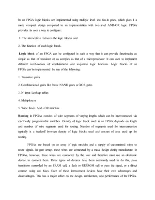
- 5. software development tools and true parallel implementation. Field Programmable Gate Array (FPGA) are a family of programmable device based on an array of configurable logic blocks (CLBs), which gives a great flexibility in prototyping, designing and development of complex hardware real time systems. The structure of a FPGA can be described as an "array of blocks" connected together via programmable interconnections. The main advantage of FPGA is the flexibility that they afford [ 3]. Xilinx Inc. introduced the world's first FPGA, the XC2064 in 1985. The XC2064 contained approximately 1000 logic gate. Since then, the gate density of Xilinx FPGAs has increased thousands times. Recently there is a lot of interest in the FPGA realization of neural networks which is reported by many researchers. Mathematical model of an artificial neuron: Mathematical model of artificial neuron Where j p is the input value and w j is the corresponding weight value, A is the output of the neuron, and f is a nonlinear activation function. Typically the activation function is chosen by the designer for specific training algorithm , and then the weights will be adjusted by some learning rule so that the neuron input / output relationship meet some specific goal. Haitham Kareem Ali and Esraa Zeki Mohammed “Design Artificial Neural Network Using FPGA” In layered neural networks, the neurons are organized in the form of layers. The neurons in a layer get inputs from the previous layer and feed their output to the next layer. These type of networks are called feed forward networks. Output connections from a neuron to the same or previous layer neurons are not permitted. The input layer is made of special input neurons, transmitting only the applied external input to their outputs. The last layer is called the output layer, and the layers other than input & output layers are called the hidden layers. In a network, if there are input and output layers only, then it is called a single layer network. Networks with one or more hidden layers are called multilayer networks.
- 6. Layered feed forward Neural Network One of the most important parts of a neuron is its activation function. The nonlinearity of the activation function makes it possible to approximate any function. In the hardware implementation concept of neural networks, it is not so easy to realize sigmoid activation functions. Special attention must be paid to an area-efficient implementation of every computational element when implementing large ANNs on digital hardware. This holds true for the nonlinear activation function used at the output of neurons. A common activation function is the sigmoid function Amitkumar B. Khonde, Yogesh Sharma, Sanjay Badjate “Implementation of Multilayer Feed Forward Neural Network using VHDL” FPGAs not only offer parallelism but also flexible designs, savings in cost and design cycle. Considering the relevance of choosing FPGA in order to implement ANNs, the purpose of our work is to describe in VHDL an ANN dedicated to be implemented on a other FPGA kits like Xilinx Spartan kit. Selecting a simple Feed Forward Neural Network dedicated composed of three neuron in input and one hidden layer with five neurons and one neuron in the output layer. Multilayer ANN
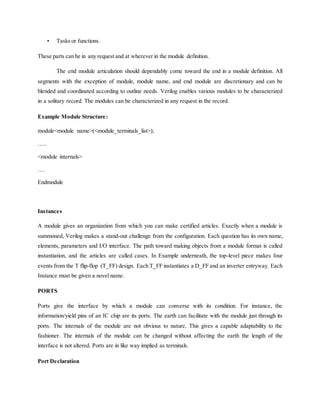
- 7. One of the most important parts of a neuron is its activation function. The nonlinearity of the activation function makes it possible to approximate any function.. This holds true for the nonlinear activation function used at the output of neurons. A common activation function is the sigmoid function Y = 1/1+ex Efficient implementation of the sigmoid function on an FPGA is a difficult challenge faced by designers. It is not suitable for direct implementation because it consists of an infinite exponential series. In most cases computationally simplified alternatives of sigmoid function are used. J. Renteria-Cedano, C. Perez-Wences, L. M. Aguilar-Lobo, J. R. Loo-Yau, J. A. Reynoso- Hernandez “A Novel Configurable FPGA Architecture for Hardware Implementation of Multilayer Feed forward Neural Networks Suitable for Digital Pre-Distortion Technique” In this paper was presented a novel configurable architecture that allows implement any Multilayer Feed forward Neural Network (MFNN) in a FPGA. The number of layers, number of neurons and threshold function of a MFNN are configured sending specific codes to the FPGA. The logical resources of the FPGA are optimized by taking into account the nature of the MFNN, this allows the programming only a single neuron to perform all the inherent mathematical operations of a MFNN. This fact represents a breakthrough for future development of DPD techniques based on artificial neural network. A typical MFNN is divided in several sections or layers, basically the first and the last layer are referred to the input and output layers, respectively, and the intermediate layers are known as hidden layers. Each layer contains a set of interconnected units called neurons in which its output depends on its input and the computational function. Aydogan Savran, Serkan unsal “Hardware implementation of a Feed forward neural network using FPGAs” Accuracy has a great impact in the learning phase; so the precision of the numbers must be as high as possible during training. However during the propagation phase, lower precisions are acceptable. The resulting errors will be small enough to be neglected especially in classification applications. In the XOR problem we applied, the input space is between –1 and 1. The training resulted in weights residing between –2 and 2. We chose 8-bit precision for the system to cover the [-2,2] range, resulting in a
- 8. precision of 1/64. Table 1 shows various numbers in this range and their 8-bit representation. To represent negative numbers, 2’s complement method is used. Data representation This paper has presented the implementation of neural networks by FPGAs. The proposed network architecture is modular, being possible to easily increase or decrease the number of neurons as well as layers. FPGAs can be used for portable, modular, and reconfigurable hardware solutions for neural networks, which have been mostly used to be realized on computers until now. ARTIFICIAL NEURAL NETWORKS
- 9. Artificial neural networks are inspired by the biological neural systems. The transmission of signals in biological neurons through synapses is a complex chemical process in which specific transmitter substances are released from the sending side of the synapse. The effect is to raise or lower the electrical potential inside the body of the receiving cell. If this potential reaches a threshold, the neuron fires. It is this characteristic of the biological neurons that the artificial neuron model proposed by McCulloch Pitts attempts to reproduce. Following neuron model shown in Fig. 1 is widely used in artificial neural networks with some variations. The artificial neuron given in this figure has N inputs, denoted as p1, p2...pN. Each line connecting these inputs to the neuron is assigned a weight, denoted as w1, w2,…, wN respectively. The activation, a, determines whether the neuron is to be fired or not. It is given by the formula. Neuron Architecture In this work we chose multiply and accumulate structure for neurons. In this structure there is one multiplier and one accumulator per neuron. The inputs from previous layer neurons enter the neuron serially and are multiplied with their corresponding weights. Every neuron has its own weight storage ROM. Multiplied values are summed in an accumulator. The processes are synchronized to clock signal. The number of clock cycles for a neuron to finish its work, equals to the number of connections from the previous layer. The accumulator has a load signal, so that the bias values are loaded to all neurons at start- up. This neuron architecture is shown in Figure 1. In this design the neuron architecture is fixed throughout the network and is not dependent on the number of connections.
- 10. Figure 1. Block diagram of a single neuron. Layer Architecture In fist Implementation of an ANN layer they take an input from their common input line, multiply it with the corresponding weight from their weight ROM and accumulate the product. If the previous layer has 3 neurons, present layer takes and processes these inputs in 3 clock cycles. After these 3 clock cycles, every neuron in the layer has its net values ready. Then the layer starts to transfer these values to its output one by one for the next layer to take them successively by enabling corresponding neuron’s three-state output. The block diagram of a layer architecture including 3 neurons is shown in Figure below. Since only one neuron’s output have to be present at the layer’s output at a time, instead of implementing an activation function for each neuron it is convenient to implement one activation function for each layer. In this layer structure pipelining is also possible. A new input pattern can enter the network while another is propagating through the layers.
- 11. In our design an ANN layer has one input, which is connected to all neurons in this layer. But previous layer may have several outputs depending on the number of neurons it has. Each input to the layer coming from the previous layer is fed successively at each clock cycle. All of the neurons in the layer operate parallel.
- 12. Fig.2. Layered feed-forward neural network A Neuron-computing system is made up of artificial neurons and a huge number of interconnections between them.Fig.2 show architecture of feed forward neural network. In layered neural network, the neurons are organized in the form of layers. The neurons in a layer get inputs from the previous layer and feed their output to the next layer. These types of networks are called feed-forward networks. Output connections from a neuron to the same or previous layer neurons are not permitted. The input layer is made of special input neurons, transmitting only the applied external input to their outputs. In a network, if there are input and output layers only, then it is a single layer network. Networks with one or more hidden layers are called multilayer networks. They take an input from their common input line, multiply it with the corresponding weight from their weight ROM and accumulate the product. If the previous layer has 3 neurons, present layer takes and processes these inputs in 3 clock cycles. After these 3 clock cycles, every neuron in the layer has its net values ready. Then the layer starts to transfer these values to its output one by one for the next layer to take them successively by enabling corresponding neuron’s three-state output. The block diagram of a layer architecture including 3 neurons is shown in Figure 3.
- 13. Since only one neuron’s output have to be present at the layer’s output at a time, instead of implementing an activation function for each neuron it is convenient to implement one activation function for each layer. In this layer structure pipelining is also possible. A new input pattern can enter the network while another is propagating through the layers. Network Architecture The control signals in the system are generated by a state machine. This state machine is responsible of controlling all of the operations in the network. First it activates the load signals of the neurons and the neurons load their bias values. Then hidden layer is enabled for 3 clock cycles, and then the output layer consisting of a single neuron is enabled for 5 clock cycles. Figure 3. Block diagram of a layer consisting of 3 neurons. Out enable signals are also activated by this state machine. The state machine is designed using generic VHDL coding so that it can easily be applied to different network configurations. The state machine generates weight ROM addresses in a priory determined sequence so that same address lines can be used by all of the neurons in the system. Input RAM also uses this address line. Once the input RAM is loaded
- 14. by input values using the switches on the board, the propagation phase starts and the output of the network is displayed. The block diagram of the network is shown in Figure 4. Figure 4. Block diagram of the 3-5-1 network. Neural Network Types Perceptron The Perceptron neuron was introduced 1958 by Frank Rosenblatt. It is the oldest neuronal model which was also used in commercial applications. Perceptrons could not be connected to multi-layered networks because their training was not possible yet. The neuron itself implements a threshold function with binary inputs and outputs. It is depicted in Figure 7.
- 15. Figure 7 Perceptron neuron Adaline, Madaline The ADALINE is also a single neuron which was introduced 1960 by Bernhard Widrow. “ADALINE” stands for “Adaptive Linear Neuron” and “Adaptive Linear Element”, respectively. The ADALINE neuron implements a threshold function with bipolar output. Later it was enhanced to allow continuous outputs. Inputs are usually bipolar, but binary or continuous inputs are also possible. In functionality it is comparable to the Perceptron. “MADALINE” spells “Many ADALINEs” – many ADALINEs whose outputs are combined by a mathematical function. This approach is visualised in Figure 2.7. MADALINE is no multi-layered network, because the connections do not carry weight values. Still, through the combination of several linear classification borders more complex problems can be handled. ADALINE neuron as adaptive filter MADALINE Back propagation
- 16. The term “Back propagation” names the network topology and the corresponding learning method. In literature, the network itself is often called “Multi-Layer Perceptron Network” The most popular neural network type is the Back propagation network. It is widely used in many different fields of application and has a high commercial significance. Back propagation was first introduced by Paul Werbos Hopfield The Hopfield network was presented 1982 by John Hopfield. It is the most popular neural network for associative storage. It memorizes a number of samples which can also be recalled by disturbed versions of themselves Hopfield network ART Adaptive Resonance Theory (ART) is a group of networks which have been developed by Stephen Grossberg and Gail Carpenter since 1976. ART networks learn unsupervised by subdividing the input samples into categories. Most unsupervised learning methods suffer the drawback that they tend to forget old samples, when new ones are learned.
- 17. ART Structure Cascade Correlation The Cascade Correlation network was developed in 1990 by Scott E. Fahlman and Christian Lebiere [13]. It is an example of a growing network structure. Usually it is difficult to find a suitable network structure for a given problem. In the majority of cases try-and-error is used, possibly supported by heuristic methods. In Cascade Correlation networks the structure is part of the training process. FIELD PROGRAMMABLE GATE ARRAYS FPGA provide the next generation in the programmable logic devices. The word Field in the name refers to the ability of the gate arrays to be programmed for a specific function by the user instead of by the manufacturer of the device. The word Array is used to indicate a series of columns and rows of gates that can be programmed by the end user. As compared to standard gate arrays, the field programmable gate arrays are larger devices. The basic cell structure for FPGA is somewhat complicated than the basic cell structure of standard gate array. The programmable logic blocks of FPGA are called Configurable Logic Block (CLB).
- 18. A configurable program stored in internal static memory cells determines the logic functions and the interconnections. The configurable data is loaded into the device during power-up reprogramming function. FPGA devices are customized by loading configuration data into internal memory cells. The FPGA device can either actively read its configuration data out of an external serial or byte-wide parallel PROM (master modes), or the configuration data can be written to the FPGA devices (slave and peripheral modes). Architecture of FPGA The fig below shows the general structure of FPGA chip. It consists of a large number of programmable logic blocks surrounded by programmable I/O block. The programmable logic blocks of FPGA are smaller and less capable than a PLD, but an FPGA chip contains a lot more logic blocks to make it more capable. As shown in fig.1 the logic blocks are distributed across the entire chip. These logic blocks can be interconnected with programmable inter connections. Xilinx, Inc inverted FPGAs, and in this section we will see the FPGA architecture used by Xilinx. The programmable logic blocks in the Xilinx family of FPGAs are called Configurable Logic Blocks (CLBs).The Xilinx architecture uses, CLBs, I/O blocks switch matrix and an external memory chip to realize a logic function. It uses external memory to store the interconnection information. Therefore, the device can be reprogrammed by simply changing the configuration data stored in the memory. Architecture of FPGA
- 19. An FPGA is a device that contains a matrix of reconfigurable gate array logic circuitry. When a FPGA is configured, the internal circuitry is connected in a way that creates a hardware implementation of the software application. Unlike processors, FPGAs use dedicated hardware for processing logic and do not have an operating system. FPGAs are truly parallel in nature so different processing operations do not have to compete for the same resources. As a result, the performance of one part of the application is not affected when additional processing is added. Also, multiple control loops can run on a single FPGA device at different rates. FPGA-based control systems can enforce critical interlock logic and can be designed to prevent I/O forcing by an operator. However, unlike hard-wired printed circuit board (PCB) designs which have fixed hardware resources, FPGA-based systems can literally rewire their internal circuitry to allow reconfiguration after the control system is deployed to the field. FPGA devices deliver the performance and reliability of dedicated hardware circuitry. A single FPGA can replace thousands of discrete components by incorporating millions of logic gates in a single integrated circuit (IC) chip. The internal resources of an FPGA chip consist of a matrix of configurable logic blocks (CLBs) surrounded by a periphery of I/O blocks shown in Fig. 20.1. Signals are routed within the FPGA matrix by programmable interconnect switches and wire routes. Internal Structure of FPGA
- 20. In an FPGA logic blocks are implemented using multiple level low fan-in gates, which gives it a more compact design compared to an implementation with two-level AND-OR logic. FPGA provides its user a way to configure: 1. The intersection between the logic blocks and 2. The function of each logic block. Logic block of an FPGA can be configured in such a way that it can provide functionality as simple as that of transistor or as complex as that of a microprocessor. It can used to implement different combinations of combinational and sequential logic functions. Logic blocks of an FPGA can be implemented by any of the following: 1. Transistor pairs 2. Combinational gates like basic NAND gates or XOR gates 3. N-input Lookup tables 4. Multiplexers 5. Wide fan-in And - OR structure. Routing in FPGAs consists of wire segments of varying lengths which can be interconnected via electrically programmable switches. Density of logic block used in an FPGA depends on length and number of wire segments used for routing. Number of segments used for interconnection typically is a tradeoff between density of logic blocks used and amount of area used up for routing. FPGAs are based on an array of logic modules and a supply of uncommitted wires to route signals. In gate arrays these wires are connected by a mask design during manufacture. In FPGAs, however, these wires are connected by the user and therefore must use an electronic device to connect them. Three types of devices have been commonly used to do this, pass transistors controlled by an SRAM cell, a flash or EEPROM cell to pass the signal, or a direct connect using anti fuses. Each of these interconnect devices have their own advantages and disadvantages. This has a major affect on the design, architecture, and performance of the FPGA.
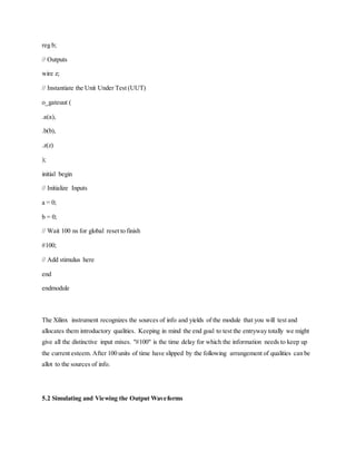
- 21. Classification of FPGAs on user programmable switch technology is given in Fig below shown below. FPGA Classification on user programmable technology FPGAs consist of three basic blocks that are configurable logic blocks, in-out blocks and connection blocks. Logic blocks perform logic function. Connection blocks connect logic blocks with in-out blocks. These structures consist of routing channels and programmable switches. Routing process is effectively connection logic blocks exist different distance the others [6]. FPGAs are chosen for implementation ANNs with the following reason: They can be applied a wide range of logic gates starting with tens of thousands up to few millions gates. They can be reconfigured to change logic function while resident in the system. FPGAs have short design cycle that leads to fairly inexpensive logic design. FPGAs have parallelism in their nature. Thus, they have parallel computing environment and allows logic cycle design to work parallel. They have powerful design, programming and syntheses tools. The architecture of ANNs must be specified with schematic or algorithmic at first step of FPGAs based system design. When ANNs based FPGAs system design specify the architecture of ANNs from a symbolic level. This level allows us using VHDL which stands for VHSIC (Very High Speed Integrated Circuit) Hardware Programming Language. VHDL allows many levels of abstractions, and permits accurate description of electronic components ranging from
- 22. simple logic gates to microprocessors. VHDL have tools needed for description and simulation which leads to a lower production cost. Fpga implementation OVERVIEW OF VHDL VHDL is language meant for describing digital electronics system. In its simplest form, the description of component in VHDL consists of an interface specification and an architectural specification. The interface description begins with the ENTITY keyword and contains the input- output ports of the component. The name of the component comes after the ENTITY keyword and is followed by IS, which is also a VHDL keyword. The description of the internal implementation of an entity is called an architecture body of the entity. There may be number of different architecture bodies of an interface to an entity corresponding to alternative implementations that perform the same function. After describing a digital system in VHDL, simulation of the VHDL code has to be carried out for two reasons. First, we need to verify whether the VHDL code correctly implements the intended design. Second, we need to verify that the design meets its specification. The simulation is used to test the VHDL code by writing
- 23. test bench model. A test bench model that is employed to exercise and verify the correctness of a hardware model and it can be described in the same language. Some synthesis tools are capable of implementing the digital system described by VHDL code using a PGA (programmable gate array) or CPLD (complex programmable logic devices), they are more flexible and more versatile and can be used to implement a complete digital system on a single chip. The user can program the functions realized by each logic cell and the connections between the cells. Such PGAs are often called FPGAs (field programmable logic array)
- 24. VERY LARGE SCALE INTEGRATION 5.1 HISTORYOF VERILOG Verilog was started in the year 1984 by Gateway Design Automation Inc as a restrictive hardware showing tongue. It is presumed that the principal vernacular was created by taking components from the most pervasive HDL tongue of the time, called HiLo, and also from standard scripting dialects, for instance, C. Around then, Verilog was not systematized and the tongue changed itself in each one of the updates that turned out inside 1984 to 1990. Verilog test framework at first used as a piece of 1985 and grew impressively through 1987. The utilization of Verilog test framework sold by Gateway. The central genuine enlargement of Verilog can't avoid being Verilog-XL, which incorporated a few highlights and executed the famous "XL count" which is an extraordinarily compelling procedure for doing portal level reenactment. Later 1990, Cadence Design System, whose basic thing around then included thin film handle test framework, secured Gateway Automation System, close by other Gateway things., Cadence now transform into the proprietor of the Verilog vernacular, and continued advancing Verilog as both a lingo and a test framework. Meanwhile, Synopsys was exhibiting the top-down blueprint method, using Verilog. This was a powerful mix. In 1990, Cadence dealt with the Open Verilog International (OVI), and in 1991 gave it the documentation for the Verilog Hardware Description Language. This was the event which "opened" the tongue. 5.2 BASIC CONCEPTS Hardware Description Language Two things recognize a HDL from a straight dialect like "C": Simultaneousness: • The capacity to do a few things at the same time i.e. distinctive code-pieces can run simultaneously. Timing: • Ability to speak to the progression of time and succession occasions in like manner
- 25. VERILOG Introduction • Verilog HDL is a Hardware Description Language (HDL). • A Hardware Description Language is a tongue used to delineate a propelled system; one may depict a mechanized structure at a couple levels. • An HDL may portray the configuration of the wires, resistors and transistors on an Integrated Circuit (IC) chip, i.e., the switch level. • It may delineate the reasonable entryways and flip tumbles in a propelled structure,i.e., the gateway level. • An altogether more raised sum portrays the registers and the trades of vectors of information between registers. This is known as the Register Transfer Level (RTL). • Verilog reinforces these levels. A capable element of the Verilog HDL is that you can utilize a similar dialect for depicting, testing and troubleshooting your framework. VERILOG Features Strong Background: • Supported by OVI, and organized in 1995 as IEEE sexually transmitted malady 1364 Current support: • Fast generation and capable synthesis(85% were used as a piece of ASIC foundries by EE TIMES) General: • Allows entire process in one diagram condition (tallying examination and affirmation) Extensibility: • Verilog PLI that considers development of Verilog limits Design Flow The regular plan stream is appeared in figure Design Specification
- 26. • Specifications are made first-Requirement/needs about the wander • Describe the convenience general building of the propelled circuit to be plot. • Specification: Word processor like Word, K writer, Abi Word and for drawing waveform use devices like wave past or test bencher or Word. RTL Description • Conversation of Specification in coding position utilizing CAD Tools. Coding Styles: • Gate Level Modeling • Data Flow Modeling • Behavioral Modeling RTL Coding Editor: Vim, Emacs, 26ontext, HDL TurboWriter
- 27. Figure 5.1 VLSI Design Flow Functional Verification &Testing • Comparing the coding with the judgments. • Testing the Process of coding with contrasting data sources and yields. • If testing crashes and burns – toward the day's end check the RTL Description. • Simulation: Modelsim, VCS, Verilog-XL, Xilinx.
- 28. Figure 5.2 Simulation Output View of 4:1 MUX Using Modelsim Wave form Viewer Logic Synthesis • Conversation of RTL depiction into Gate level - Net rundown shape. • Description of the circuit as far as entryways and associations. • Synthesis: Design Compiler, FPGA Compiler, Synplify Pro, Leonardo Spectrum, Altera and Xilinx . Figure 5.3 Synthesis of 4:1 MUX Using Leonardo Spectrum Logical Verification and Testing Functional Checking of HDL coding by reproduction and combination. In the event that falls flat – check the RTL depiction.
- 29. Floor Planning Automatic Place and Route • Creation of Layout with the relating entryway level Net rundown. • Arrange the squares of the net rundown on the chip • Place and Route: For FPGA utilize FPGA' sellers P&R device. ASIC devices require costly P&R apparatuses like Apollo. Understudies can utilize LASI, Magic Physical Layout • Physical setup is the route toward changing a circuit delineation into the physical outline, which depicts the position of cells and courses for the interconnections between them. Layout Verification • Verifying the physical plan structure. • If any change –once again check Floor Planning Automatic Place and Route and RTL Description. Implementation • Final organize in the plan procedure. • Implementation of coding and RTL as IC. 5.3 Design Hierarchies Bottom up Design The Traditional procedure for electronic plan is base up. Each outline is performed at the gateway level utilizing the standard sections .With developing multifaceted nature of new plans this approach is about difficult to keep up. It offers approach to manage new basic, diverse leveled orchestrate systems. Without these new course of action hones it is difficult to deal with the new multifaceted nature
- 30. Figure 5.4 Bottom Up Design Top-Down Design A genuine best down outline permits early testing, clear change of various movements, a sorted out structure plan and offers different unmistakable focal core interests. Notwithstanding, it is astoundingly hard to bring after an unadulterated top-down structure. Subsequently of this reality most plans are blend of both the procedures. Executing some key portions of both game plan styles Figure 5.5 Top-Down Design Lexical Conventions
- 31. The fundamental lexical traditions utilized by Verilog HDL are like those in the C programming dialect. Verilog contains a surge of tokens. Tokens can be remarks, delimiters, numbers, strings, identifiers, and catchphrases. Verilog HDL is a case-touchy dialect. All watchwords are in lower case. Whitespace Void area can contain the characters for spaces,tabs,newlines, and frame bolsters. These characters are overlooked with the exception of when they serve to isolate different tokens. Nonetheless, spaces and tabs are critical in strings. Void area characters are: • Blank spaces (b) • Tabs(t) • Carriage returns(r) • New-line (n) • Form-sustains (a) Comments Remarks can be embedded in the code for meaningfulness and documentation. There are two structures to present remarks. • Single line remarks start with the token/and end with a carriage return • Multi line remarks start with the token/* and end with the token */ Identifiers and Keywords Identifiers are names used to give a question, for example, an enroll or a capacity or a module, a name so it can be referenced from different places in a depiction. Watchwords are held to characterize the dialect develops. • Identifiers must start with an alphabetic character or the underscore character (a-z,A-Z)
- 32. • Identifiers may contain alphabetic characters,numeric characters,the underscore,and the dollar sign (a-z A-Z 0-9 _ $ ) • Identifiers can be up to 1024 characters in length. • Keywords are in lowercase. Examples oflegal identifiers • data_input mu • clk_inputmy$clk • i386 Examples ofkeywords • always • begin • end Escaped Identifiers Verilog HDL empowers any character to be used as a piece of an identifier by making tracks in an opposite direction from the identifier. Escaped identifiers give a strategies for including any of the printable ASCII characters in an identifier (the decimal qualities 33 through 126, or 21 through 7E in hexadecimal). • Escaped identifiers begin with the diagonal accentuation line ( ) • Entire identifier is escaped by the diagonal accentuation line. • Escaped identifier is finished by clear range (Characters,for instance, commas, nooks, and semicolons end up being a bit of the escaped identifier unless gone before by a void region) • Terminate escaped identifiers with clear range, by and large characters that should take after the identifier are considered as a noteworthy part of it. Numbers in Verilog Numbers in Verilog can be resolved steady numbers in decimal, hexadecimal, octal, or twofold association. Negative numbers are addressed in 2's supplement shape. Right when used as a piece of a
- 33. number, the question mark (?) character is the Verilog elective for the z character. The underscore character (_) is true blue wherever in a number except for as the central character, where it is slighted. Integer Numbers Verilog HDL allows entire number numbers can be resolved as • Sized or unsized numbers (Unsized size is 32 bits) • In a radix of twofold, octal, decimal, or hexadecimal • Radix and hex digits (a,b,c,d,e,f) are case brutal • Spaces are allowed between the size, radix and regard Entire number numbers are addressed as <size>'<base format><number><size>is made just in decimal and shows the amount of bits in the number. Legitimate base setups are decimal ('d or 'D), hexadecimal ('h or 'H), combined ('b or'B) and octal ('o or 'O). the number is demonstrated as consecutive digits from 0,1,2,3,4,5,6,7,8,9,a,b,c,d,e,f. only a subset of these digits is legal for a particular base. Uppercase letters are authentic for number detail. 4'b1101 –this is a 4-bit twofold number 12'hcba – this is a 12-bit hexadecimal number 16'd165 – this is a 16-bit decimal number 8'o43-this is 8 bit octal number Real Numbers • Verilog underpins genuine constants and factors • Verilog changes over genuine numbers to whole numbers by adjusting • Real Numbers can not contain "Z" and "X" • Real numbers might be determined in either decimal or logical documentation • < esteem >.< esteem >
- 34. • < mantissa >E< type > • Real numbers are adjusted off to the closest whole number when relegating to a whole number. Example Signed and Unsigned Number Verilog supports both sorts of numbers, however with particular controls. Like in C lingo Verilog don't have int and unint sorts to state if a number is stamped entire number or unsigned number. Any number that does not have negative sign prefix is a positive number. Or, on the other hand indirect way would be "Unsigned". Negative numbers can be controlled by putting a less sign before the size for a relentless number, hence they wind up obviously stamped numbers. Verilog inside addresses negative numbers in 2's supplement sort out. An optional stamped specifier can be incorporated for checked number juggling. Example Strings A string is a succession of characters that are encased by twofold quotes. The limitation on a string is that it must be contained on a solitary line, that is, without a carriage return. It can't be on numerous lines, Strings are dealt with as a succession of one-byte ASCII values. Examples “Hi good morning”
- 35. “c/d” “dd+d” Data types Each flag has an information sort related with it: • Explicitly proclaimed with an assertion in your Verilog code. • Implicitly announced with no statement when used to associate basic building obstructs in your code. Understood assertion is dependably a net sort "wire" and is one piece wide. Data Types Value set Verilog underpins four qualities and eight qualities to show the usefulness of genuine equipment. The four levels are recorded in table Value level Condition in hardware circuits • 0 rationale zero, false condition • 1 rationale one, genuine condition • x obscure esteem • z High impedance, skimming state Register Data Types • Registers store the last esteem appointed to them until another task proclamation changes their esteem. • Registers speak to information stockpiling builds. • You can make regs clusters called recollections. • Register information sorts are utilized as factors in procedural pieces. • A enlist information sort is required if a flag is doled out an incentive inside a procedural piece • Proceduralsquares start with watchword beginning and dependably.
- 36. Example Vectors Nets or reg data sorts can be declared as vectors. In the occasion that bit width is not demonstrated, the default is scalar (1-bit).Vectors can be reported at [high#: low#] or [low#: high#], yet the left number in the squared areas is reliably the most significant bit of the vector. Integer, Real and Time Register Data Types Integer An entire number is an all around helpful enroll data sort used for controlling sums. Entire numbers are articulated by the catchphrase number. Despite the way that it is possible to use reg as a generally valuable variable, it is more useful to announce an entire number variable for purposes, for instance, checking. The default width for an entire number is the host-machine word measure, which is use specific however is no under 32 bits. Registers articulated as data sort reg store values as unsigned sums, however entire numbers store a motivator as stamped sums. Example number counter; //universally useful variable utilized as a counter introductory counter=-1; //A negative one is put in the counter Real Real number constants and bona fide enlist data sorts are articulated with the watchword honest to goodness. They can be resolved in decimal documentation or in intelligent documentation. Honest to goodness numbers can't have a range disclosure, and their default regard is 0. Right when a honest to goodness regard is consigned to an entire number, the bona fide number is balanced off to the nearest number. Time
- 37. Verilog diversion is done concerning reenactment time. An outstanding time select data sort is used as a piece of Verilog to store entertainment time. A period variable is announced with the watchword time. The width for time enroll data sorts is execution specific yet is no under 64 bits. The structure work $timeis summoned to get the present amusement time. Example timesave_sim_time; //characterize a period variable save_sim_time starting save_sim_time=$time; //spare the present reenactment time Arrays Arrays are permitted in Verilog for reg, whole number, time and vector enlist information sorts. Arrays are not considered genuine factors. Arrays are gotten to by <array_name>[<subscript>]. Multidimensional arrays not allowed in Verilog. Example whole number count[7:0];//a variety of 8 check factors reg bool [31:0];//cluster of 32 one-piece Boolean enlist factors whole number matrix[4:0][4:0];//illicit statement Multidimensional exhibit Memories In cutting edge propagation, one frequently needs to show select records,RAMs and ROMs. Memories are shown in Verilog essentially as an assortment of registers. Each part of the display is known as a word. Each word can be no less than one bits. It is crucial to isolate between n 1-bit registers and one n-bit select. A particular word in memory is gotten by using the address as a memory display subscript. Example reg mem1bit[0:1023]; //memory mem1bit with 1K 1-bit words reg [7:0]membyte[0:1023]; //memory membyte with 1K 8-bit words
- 38. Parameters Verilog enables constants to be characterized in a module by the watchword parameter. Parameters can't be utilized as factors. Parameter values for every module occasion can be abrogated separately at accumulate time. This permits the module occasions to be redone. Example parameterport_id = 5;/Defines a steady port_id parametercache_line_width= 256;/Constant characterizes width of store line Strings Strings can be secured in reg. The width of the select elements must be adequately gigantic to hold the string. Each character in the string takes up 8 bits (1 byte). If the width of the enroll is more critical than the measure of the string, Verilog fills bits to left of the string with zeros. If the enroll width is smaller than the string width, Verilog truncates the uttermost left bits of the string. It is always ensured to articulate that is to some degree more broad than would typically be fitting Example reg [8*81:1] string_value;/pronounce a variable that is 18 bytes wide starting string_value="hello Verilog course group";/string can be put away in factor MODULES A module in Verilog involves specific parts as showed up in figure. A module definition reliably begins with the watchword module. The module name, port rundown, port insistences, and optional parameters must begin things out in a module definition. Port rundown and port declarations are accessible just if the module has any ports to interface with the external condition. The five sections inside a module are; • Variable announcements, • Data flow articulations • Instantiation of lower modules • Behavioral blocks
- 39. • Tasks or functions. These parts can be in any request and at wherever in the module definition. The end module articulation should dependably come toward the end in a module definition. All segments with the exception of module, module name, and end module are discretionary and can be blended and coordinated according to outline needs. Verilog enables various modules to be characterized in a solitary record. The modules can be characterized in any request in the record. Example Module Structure: module<module name>(<module_terminals_list>); ….. <module internals> …. Endmodule Instances A module gives an organization from which you can make certified articles. Exactly when a module is summoned, Verilog makes a stand-out challenge from the configuration. Each question has its own name, elements, parameters and I/O interface. The path toward making objects from a module format is called instantiation, and the articles are called cases. In Example underneath, the top-level piece makes four events from the T flip-flop (T_FF) design. Each T_FF instantiates a D_FF and an inverter entryway. Each Instance must be given a novel name. PORTS Ports give the interface by which a module can converse with its condition. For instance, the information/yield pins of an IC chip are its ports. The earth can facilitate with the module just through its ports. The internals of the module are not obvious to nature. This gives a capable adaptability to the fashioner. The internals of the module can be changed without affecting the earth the length of the interface is not altered. Ports are in like way implied as terminals. Port Declaration
- 40. All ports in the rundown of ports must be proclaimed in the module. Ports can be proclaimed as takes after Verilog Keyword Type ofPort • inputInput port • outputOutput port • inout Bidirectional port Each port in the port rundown is characterized as information, yield, or inout, in light of the bearing of the port flag. Port Connection Rules One can envision a port as containing two units, one unit that is internal to the module another that is outside to the module. The inward and outside units are connected. There are models coordinating port affiliations when modules are instantiated inside different modules. The Verilog test structure dissents if any port alliance standards are hurt. These norms are pressed in figure. Port connection Rules Inputs: • Internally should be of net information sort (e.g. wire) • Externally the sources of info might be associated with a reg or net information sort Outputs: • Internally might be of net or reg information sort • Externally should be associated with a net information sort
- 41. In-outs: • Internally should be of net information sort (tri prescribed) • Externally should be associated with a net information sort (tri prescribed) Ports Connection to External Signals There are two strategies for making associations between signs determined in the module instantiation and ports in a module definition. The two techniques can't be blended. • Port by request list • Port by name Port by request list Interfacing port by request rundown is the most natural strategy for generally tenderfoots. The signs to be associated must show up in the module instantiation in an indistinguishable request from the ports in the ports list in the module definition. Sentence structure for instantiation with port request list: module_nameinstance_name(signal, signal...); From the underneath illustration, see that the outer signs a, b, out show up in the very same request as the ports a, b, out in the module characterized in viper beneath. Port by name For bigger outlines where the module have ,say 5o ports , recollecting the request of the ports in the module definition is unrealistic and blunder inclined. Verilog gave the ability to associate outer signs to ports by the port names, instead of by position. Linguistic structure for instantiation with port name: module_nameinstance_name (.port_name(signal), .port_name (flag)… ); From the beneath case,take note of that the port associations in any request the length of the port name in the module definition accurately coordinates the outside flag.
- 42. MODELING CONCEPTS Verilog is both a behavioral and a basic vernacular. Internals of every module to be depicted at four levels of reflection, ward upon the necessities of the plan. The module carries on indistinctly with the outside condition free of the level of thought at which the module is depicted. The internals of the module avoided nature. Along these lines, the level of contemplating to delineate a module can be changed with no alteration in the earth. The levels are portrayed underneath • Behavioral or algorithmic level This is the most raised measure of reflection given by Verilog HDL. A module can be executed similarly as the desired framework figuring without stress for the gear utilization purposes of intrigue. Arranging at this level is on a very basic level the same as C programming • Dataflow level At this level the module is arranged by deciding the data stream. The organizer thinks about how data streams between gear registers and how the data is dealt with in the framework. • Gate level The module is completed with respect to basis entryways and interconnections between these portals. Arrange at this level resembles depicting a layout with respect to a passage level method of reasoning diagram. • Switch level This is the most unimportant level of reflection given by Verilog. A module can be executed the degree that switches, stockpiling focus focuses, and the interconnections between them. Graph at this level requires information of switch-level execution unnoticeable segments. Verilog enables the fashioner to blend and match every one of the four levels of appearance in a plan. In the moved orchestrate gathering, the term register transfer level (RTL) is as regularly as possible utilized for a Verilog depiction that uses a blend of behavioral and data flow makes and is satisfactory to technique for thinking mix contraptions.
- 43. If an arrangement contains four modules, Verilog empowers each of the modules to be formed at a substitute level of reflection. As the arrangement grows, most modules are supplanted with door level use. Normally, the higher the level of reflection, the more versatile and advancement Independent the arrangement. As one goes bring down toward switch-level arrangement, the blueprint pushes toward getting to be advancement penniless and inflexible. A little change can realize an important number of changes in the arrangement. Differentiating the relationship and C programming and low level registering build programming. It is less difficult to program in more hoisted sum vernacular, for instance, C. The program can be adequately ported to any machine. Regardless, if the arrangement at the social event level, the program is specific for that machine and can't be adequately ported to another machine. ENTRYWAY LEVEL MODELING Verilog has worked in primitives like entryways, transmission portals, and switches. These are on occasion used as a piece of layout (RTL Coding), however are used as a piece of post mix world for showing the ASIC/FPGA cells; these cells are then used for entryway level amusement. Similarly the yield net summary arrange from the mix contraption, which is outside into the place and course gadget, is also in Verilog entryway level primitives. BEHAVIORALAND RTL MODELING Verilog gives fashioners the capacity to depict chart an incentive in an algorithmic way. In a manner of speaking, the artist depicts the lead of the circuit. In this way, behavioral showing addresses the circuit at an irregular state of thought. Organize at this level looks like C programming more than it takes after mechanized circuit outline. Behavioral Verilog makes take after C vernacular structures from different points of view. Verilog is rich in behavioral develops that outfit the fashioner with a noteworthy measure of flexibility. Operators Verilog gave a wide range of administrators sorts. Administrators can be, • Arithmetic Operators • Relational Operators • Bit-wise Operators
- 44. • Logical Operators • Reduction Operators • Shift Operators • Concatenation Operator • Replication Operator • Conditional Operator • Equality Operator Arithmetic Operators • These perform number juggling operations. The + and - can be utilized as either unary (-z) or paired (x-y) administrators. • Binary: +, - , *,/, % (the modulus administrator) • Unary: +, - (This is utilized to indicate the sign) • Integer division truncates any fragmentary part • The aftereffect of a modulus operation takes the indication of the principal operand • If any operand bit esteem is the obscure esteem x, then the whole outcome esteem is x • Register information sorts are utilized as unsigned qualities (Negative numbers are put away in two's supplement frame) Relational Operators Social administrators look at two operands and give back a solitary piece 1or 0. These administrators combine into comparators. Wire and reg factors are sure Thus (- 3'b001) = 3'b111 and (- 3d001)>3d1 10, however for whole numbers - 1< 6
- 45. • The result is a scalar esteem (illustration a < b) • 0 if the connection is false (an is greater than b) • 1 if the connection is genuine ( an is littler than b) • x if any of the operands has obscure x bits (if an or b contains X) Note: If any operand is x or z, then the consequence of that test is dealt with as false (0) Recreation Output 5 <= 10 = 1 5 >= 10 = 0 1'bx <= 10 = x 1'bz<= 10 = x Bit-wise Operators Bitwise heads play out to some degree astute operation on two operands. This take each piece in one operand and play out the operation with the looking at bit in the other operand. If one operand is shorter than the other, it will be connected on the left support zeroes to organize the length of the more broadened operand.
- 46. • Computations incorporate obscure bits, in the accompanying way: • ~x = x 0&x = 0 1&x = x&x = x 1|x = 1 0|x = x|x = x 0^x = 1^x = x^x = x 0^~x = 1^~x = x^~x = x When operands are of unequal piece length, the shorter operand is zero-filled in the most noteworthy piece positions. Logical Operators Keen managers give back a single piece 1 or 0. They are the same as bit-wise directors only for single piece operands. They can manage expressions, entire numbers or social occasions of bits, and treat all values that are nonzero as "1". Sensible managers are conventionally used as a piece of prohibitive (if ... else) declarations since they work with expressions. • Expressions associated by && and || are assessed from left to right
- 47. • Evaluation stops when the outcome is known • The result is a scalar esteem: • 0 if the connection is false • 1 if the connection is valid • x if any of the operands has x (obscure) bits Reduction Operators Diminishment administrators work on every one of the bits of an operand vector and give back a singlebit esteem. These are the unary (one contention) type of the bit-wise administrators. • Reduction administrators are unary. • They play out somewhat shrewd operation on a solitary operand to create a solitary piece result. • Reduction unary NAND and NOR administrators work as AND as well as individually, yet with their yields refuted. • Unknown bits are dealt with as portrayed some time recently Shift Operators Move administrators move the principal operand by the quantity of bits indicated by the second operand. Cleared positions are loaded with zeros for both left and right moves (There is no sign expansion).
- 48. • The left operand is moved by the quantity of bit positions given by the correct operand. • The cleared piece positions are loaded with zeroes Link Operator The link administrator joins at least two operands to shape a bigger vector. • Concatenations are communicated utilizing the prop characters { and }, with commas isolating the expressions inside. • Example: + {a, b[3:0], c, 4'b1001}/if an and c are 8-bit numbers, the outcomes has 24 bits • Unsized steady numbers are not permitted in links. • Operator Precedence Procedural Blocks
- 49. Verilog behavioral code is inside technique squares, yet there is an exemption: some behavioral code likewise exist outside methodology pieces. We can see this in detail as we gain ground. There are two sorts of procedural pieces in Verilog: • Initial: beginning pieces execute just once at time zero (begin execution at time zero). • Always: dependably pieces circle to execute again and again; as such, as the name proposes, it executes dependably. Illustration – starting moduleinitial_example(); regclk,reset,enable,data; beginning start clk = 0; reset = 0; empower = 0; information = 0; end endmodule In the above illustration, the underlying piece execution and dependably square execution begins at time 0. Continuously square sits tight for the occasion, here positive edge of clock, though introductory piece simply executed every one of the announcements inside start and end articulation, without holding up. Case – dependably modulealways_example(); regclk,reset,enable,q_in,data; continuously @ (posedgeclk)
- 50. in the event that (reset) start data<= 0; end else if (empower) start data<= q_in; end endmodule In a dependably piece, when the trigger occasion happens, the code inside start and end is executed; then by and by the dependably square sits tight for next occasion activating. This procedure of holding up and executing on occasion is rehashed till reenactment stops. 5.4 Xilinx Verilog HDL Tutorial Getting started On the off chance that you wish to wear out this instructional exercise and the lab at home, you should download and exhibit Xilinx and ModelSim. These mechanical gatherings both have free understudy varieties. You ought to finish Appendix B, C, and D in a specific demand before proceeding with this instructional exercise. Moreover in the event that you wish to buy your own particular Spartan3 board, you can do in that limit at Dig advance’s Website. Resolute offers instructive surveying. In the event that its all the same to you watch that you should download and introduce Diligent Adept programming. The thing contains the drivers for the board that you require furthermore gives the interface to program the board. 5.4.1 Introduction Xilinx Tools is a suite of programming devices utilized for the course of action of modernized circuits finished utilizing Xilinx Field Programmable Gate Array (FPGA) or Complex Programmable Logic Device (CPLD). The game plan technique includes (a) plot territory, (b) blend and utilization of the course of action, (c) utilitarian amusement and (d) testing and check. Mechanized structures can be entered in different ways utilizing the above CAD devices: utilizing a schematic passage instrument, utilizing a Hardware description Language (HDL) – Verilog or VHDL or a mix of both. In this lab we will essentially utilize the course of action stream that fuses the utilization of Verilog HDL.
- 51. The CAD contraptions draw in you to outline combinational and dynamic circuits beginning with Verilog HDL mastermind purposes of intrigue. The techniques for this course of action system are recorded underneath: • Create Verilog plan input file(s) utilizing bunch driven editorial manager. • Compile and understand the Verilog design file(s). • Create the test-vectors and repeat the outline (utilitarian reenactment) without utilizing a PLD (FPGA or CPLD). • Assign input/yield pins to execute the game plan on an objective gadget. • Download bitstream to a FPGA or CPLD contraption. • Test plot on FPGA/CPLD contraption A Verilog input record in the Xilinx programming condition includes the running with fragments: Header:module name, once-over of information and yield ports. Statements: information and yield ports, registers and wires. Technique for thinking Descriptions: conditions, state machines and premise limits. End: endmodule Every one of your courses of action for this lab must be appeared in the above Verilog input arrange. Watch that the state chart zone does not exist for combinational avocation follows. 1. Programmable Logic Device: FPGA In this lab propelled arrangements will be realized in the Basys2 board which has a Xilinx Spartan3E – XC3S250E FPGA with CP132 package. This FPGA part has a place with the Spartan gathering of FPGAs. These devices landed in an arrangement of groups. We will use devices that are packaged in 132 stick package with the going with part number: XC3S250E-CP132. This FPGA is a device with around 50K entryways. Organized information on this contraption is available at the Xilinx site. 2. Creating a NewProject
- 52. Xilinx Tools can be started by tapping on the Project Navigator Icon on the Windows desktop. This should open up the Project Navigator window on your screen. This window shows the last got the opportunity to develop. Xilinx Project Navigator window (snapshot from Xilinx ISE software) 1.1 Opening a project Select File->New Project to make another venture. This will raise another venture window on the desktop. Top off the vital sections as takes after:
- 53. New Project Initiation window (snapshot from Xilinx ISE software) Develop Name: Write the name of your new pursuit Develop Location: The file where you have to store the new pursuit (Note: DO NOT demonstrate the wander territory as an envelope on Desktop or a coordinator in the Xilinxbin index. Your H: drive is the best place to put it. The wander range way is NOT to have any spaces in it eg: C:NivashTAnew labsample exerciseso_gate is NOT to be used) Leave the top level module sort as HDL. Case:If the venture name were "o_gate", enter "o_gate" as the venture name and after that snap "Next". Tapping on NEXT ought to raise the accompanying window:
- 54. Gadget and Design Flow of Project (preview from Xilinx ISE programming) For each of the properties given underneath, tap on the "esteem" range and select from the rundown of qualities that show up. • Device Family: Family of the FPGA/CPLD utilized. In this lab we will utilize the Spartan3E FPGA's. • Device: The quantity of the genuine gadget. For this lab you may enter XC3S250E (this can be found on the connected prototyping board) • Package:The kind of bundle with the quantity of pins. The Spartan FPGA utilized as a part of this lab is bundled in CP132 bundle. • Speed Grade: The Speed review is "- 4". • Synthesis Tool: XST [VHDL/Verilog]
- 55. • Simulator: The apparatus used to reproduce and confirm the usefulness of the outline. Modelsim test system is coordinated in the Xilinx ISE. Consequently pick "Modelsim-XE Verilog" as the test system or even Xilinx ISE Simulator can be utilized. • Then tap on NEXT to spare the sections. All venture records, for example, schematics, netlists, Verilog documents, VHDL records, and so forth. Will be put away in a subdirectory with the venture name. A venture can just have one top level HDL source document (or schematic). Modules can be added to the venture to make a particular, various leveled outline. With a specific end goal to open a current venture in Xilinx Tools, select File->Open Project to demonstrate the rundown of tasks on the machine. Pick the venture you need and snap OK. Tapping on NEXT on the above window raises the accompanying window: Make New source window (preview from Xilinx ISE programming) If making another source record, Click on the NEW SOURCE. 1.2 Creating a Verilog HDL input petition for a combinational rationale plan In this lab we will enter a plan utilizing a basic or RTL depiction utilizing the Verilog HDL. You can make a Verilog HDL input record (.v document) utilizing the HDL Editor accessible in the Xilinx ISE Tools (or any content tool). In the past window, tap on the NEW SOURCE A window flies up as appeared in Figure 4. (Note: "Add to venture" alternative is chosen as a matter of course. On the off chance that you don't choose it then you should add the new source record to the venture physically.)
- 56. Creating Verilog-HDL source file (snapshot from Xilinx ISE software) Select Verilog Module and in the "Document Name:" region, enter the name of the Verilog source record you will make. Likewise ensure that the alternative Add to venture is chosen so that the source require not be added to the venture once more. At that point tap on Next to acknowledge the sections. This flies up the accompanying window. Define Verilog Source window (snapshot from Xilinx ISE software)
- 57. In the Port Name segment, enter the names of all info and yield sticks and indicate the Direction as needs be. A Vector/Bus can be characterized by entering proper piece numbers in the MSB/LSB segments. At that point tap on Next>to get a window demonstrating all the new source data. On the off chance that any progressions are to be made, simply tap on <Back to backpedal and roll out improvements. In the case of everything is adequate, tap on Finish > Next > Next > Finish to proceed. New Project Information window (depiction from Xilinx ISE programming) When you tap on Finish, the source record will be shown in the sources window in the Project Navigator. On the off chance that a source must be evacuated, perfectly tap on the source record in the Sources in Project window in the Project Navigator and select Removein that. At that point select Project - > Delete Implementation Data from the Project Navigator menu bar to expel any related records. 1.2 Editing the Verilog source document The source document will now be shown in the Project Navigator window. The source document window can be utilized as a content manager to roll out any fundamental improvements to the source record. All the info/yield pins will be shown. Spare your Verilog program intermittently by choosing the File->Save
- 58. from the menu. You can likewise alter Verilog programs in any content manager and add them to the venture catalog utilizing "Include Copy Source". Verilog Source code editor window in the Project Navigator (from Xilinx ISE software) Adding Logic in the generated Verilog Source code template: A short Verilog Tutorial is accessible in Appendix-A. Thus, the dialect language structure and development of rationale conditions can be alluded to Appendix-A. The Verilog source code layout produced demonstrates the module name, the rundown of ports and furthermore the announcements (input/yield) for each port. Combinational rationale code can be added to the verilog code after the statements and before the endmodule line. For instance, a yield z in an OR door with sources of info an and b can be depicted as, Assign z = a | b;
- 59. Keep in mind that the names are case delicate. Different develops for demonstrating the rationale work: A given rationale capacity can be displayed from multiple points of view in verilog. Here is another case in which the rationale capacity, is executed as a truth table utilizing a case proclamation: moduleor_gate(a,b,z); input a; input b; yield z; reg z; continuously @(a or b) start case ({a,b}) 00: z = 1'b0; 01: z = 1'b1; 10: z = 1'b1; 11: z = 1'b1; endcase end endmodule Assume we need to depict an OR door. It should be possible utilizing the rationale condition as appeared in Figure 9a or utilizing the case articulation as appeared in Figure. These are only two case develops to plan a rationale work. Verilog offers various such builds to productively demonstrate plans. A short instructional exercise of Verilog is accessible in Appendix-A.
- 60. OR gate description using assign statement (snapshot from Xilinx ISE software) 2. Synthesis and Implementation ofthe Design The plan must be orchestrated and executed before it can be checked for rightness, by running practical reenactment or downloaded onto the prototyping board. With the top-level Verilog document opened (should be possible by double tapping that record) in the HDL proofreader window in the correct portion of the Project Navigator, and the perspective of the venture being in the Module see , the actualize outline alternative can be found in the process see. Outline passage utilities and Generate Programming File choices can likewise be found in the process see. The previous can be utilized to incorporate client requirements, assuming any and the last will be talked about later. To incorporate the outline, double tap on the Synthesize Design alternative in the Processes window. To actualize the outline, double tap the Implement plan alternative in the Processes window. It will experience steps like Translate, Map and Place and Route. On the off chance that any of these means wasn't possible or finished with mistakes, it will put a X check before that, generally a tick stamp will be put after each of them to demonstrate the effective fulfillment. On the off chance that everything is done effectively, a tick check will be put before the Implement Design alternative. On the off chance that there are notices, one can see check before the choice showing that there are a few notices. One can take a gander at the notices or mistakes in the Console window exhibit at the base of the Navigator window.
- 61. Each time the outline document is spared; every one of these imprints vanish requesting a crisp assemblage. Implementing the Design (snapshot from Xilinx ISE software) The schematic chart of the combined verilog code can be seen by double tapping View RTL Schematic under Synthesize-XST menu in the Process Window. This would be a helpful approach to troubleshoot the code if the yield is not meeting our determinations in the proto sort board. By double tapping it opens the top level module demonstrating just input(s) and output(s) as demonstrated as follows.
- 62. Top Level Hierarchy of the design By double clicking the rectangle, it opens the realized internal logic as shown below. Realized logic by the XilinxISE for the verilog code 5. Functional Simulation of Combinational Designs 5.1 Adding the testvectors
- 63. To check the usefulness of a plan, we need to apply test vectors and mimic the circuit. Keeping in mind the end goal to apply test vectors, a test seat document is composed. Basically it will supply every one of the contributions to the module outlined and will check the yields of the module. Case: For the 2 information OR Gate, the means to create the test seat is as per the following: In the Sources window (upper left corner) right tap on the document that you need to create the test seat for and select 'New Source' Give a name to the test seat in the document name content box and select 'Verilog test apparatus' among the record sorts in the rundown on the correct side as appeared in figure. Adding test vectors to the design (snapshot from Xilinx ISE software) Click on ‘Next’ to proceed. In the next window select the source file with which you want to associate the test bench.
- 64. Associating a module to a testbench (snapshot from Xilinx ISE software) Click on Next to proceed. In the next window click on Finish. You will now be provided with a template for your test bench. If it does not open automatically click the radio button next to Simulation . You should now be able to view your test bench template. The code generated would be something like this: moduleo_gate_tb_v; // Inputs reg a;
- 65. reg b; // Outputs wire z; // Instantiate the Unit Under Test (UUT) o_gateuut ( .a(a), .b(b), .z(z) ); initial begin // Initialize Inputs a = 0; b = 0; // Wait 100 ns for global reset to finish #100; // Add stimulus here end endmodule The Xilinx instrument recognizes the sources of info and yields of the module that you will test and allocates them introductory qualities. Keeping in mind the end goal to test the entryway totally we might give all the distinctive input mixes. "#100" is the time delay for which the information needs to keep up the current esteem. After 100 units of time have slipped by the following arrangement of qualities can be allot to the sources of info. 5.2 Simulating and Viewing the Output Waveforms
- 66. Presently under the Processes window (ensuring that the test bench record in the Sources window is chosen) extend the ModelSim test system Tab by tapping on the add sign alongside it. Double tap on Simulate Behavioral Model. You will most likely get a complier blunder. This is nothing to stress over – reply "No" when inquired as to whether you wish to prematurely end reproduction. This ought to make ModelSim open. Sit tight for it to finish execution. In the event that you wish to not get the compiler mistake, right tap on Simulate Behavioral Model and select process properties. Stamp the checkbox beside "Disregard Pre-Complied Library Warning Check". 5.3 Saving the simulation results To spare the reenactment comes about, Go to the waveform window of the Modelsim test system, Click on File - > Print to Postscript - > give wanted filename and area. Take note of that as a matter of course,the waveform is "zoomed in" to the nanosecond level. Utilize the zoom controls to show the whole waveform. Else a typical print screen alternative can be utilized on the waveform window and in this manner put away in Paint.