


![81
A simple digital circuit With comparatively larger circuits, the task mostly reduces to one of identifying the set of ICs necessary for the job and interconnecting; rarely does one have to resort to a micro level design [Wakerly]. The accepted approach to digital design here is a mix of the top-down and bottom-up approaches as follows [Hill & Peterson]: • Decide the requirements at the system level and translate them to circuit requirements. • Identify the major functional blocks required like timer, DMA unit, register file etc., and say as in the design of a processor. • Whenever a function can be realized using a standard IC, use the same –for example programmable counter, mux, demux, etc. • Whenever the above is not possible, form the circuit to carry out the block functions using standard SSI – for example gates, flip-flops, etc. • Use additional components like transistor, diode, resistor, capacitor, etc., wherever essential.
Once the above steps are gone through, a paper design is ready. Starting with the paper design, one has to do a circuit layout. The physical location of all the components is tentatively decided; they are interconnected and the „circuit-onpaper‟ is made ready. Once a paper design is done, a layout is carried out and a net-list prepared. Based](https://image.slidesharecdn.com/fpgaimplementationofsoftdecisionlowpowerconvolutionaldecoderusingviterbialgorithm-141112050302-conversion-gate02/85/Fpga-implementation-of-soft-decision-low-power-convolutional-decoder-using-viterbi-algorithm-81-320.jpg)

![83
• Overload: Some signals may be overloaded to such an extent that the signal transition may be unduly delayed or even suppressed. The problem manifests as reflections and erratic behaviour in some cases (The signal has to be suitably buffered here.). In fact, overload on a signal can lead to timing mismatches. The above have to be carried out after completion of the prototype PCB manufacturing; it involves cost, time, and also a redesigning process to develop a bug free design. VLSI DESIGN The complexity of VLSI‟s being designed and used today makes the manual approach to design impractical. Design automation is the order of the day. With the rapid technological developments in the last two decades, the status of VLSI technology is characterized by the following [Wai-kai, Gopalan]: • A steady increase in the size and hence the functionality of the ICs. • A steady reduction in feature size and hence increase in the speed of operation as well as gate or transistor density. • A steady improvement in the predictability of circuit behaviour. • A steady increase in the variety and size of software tools for VLSI design. The above developments have resulted in a proliferation of approaches to VLSI design. We briefly describe the procedure of automated design flow [Rabaey, Smith MJ]. The aim is more to bring out the role of a Hardware Description Language (HDL) in the design process. An abstraction based model is the basis of the automated design.](https://image.slidesharecdn.com/fpgaimplementationofsoftdecisionlowpowerconvolutionaldecoderusingviterbialgorithm-141112050302-conversion-gate02/85/Fpga-implementation-of-soft-decision-low-power-convolutional-decoder-using-viterbi-algorithm-83-320.jpg)


![88
Optimization The circuit at the gate level – in terms of the gates and flip-flops – can be redundant in nature. The same can be minimized with the help of minimization tools. The step is not shown separately in the figure. The minimized logical design is converted to a circuit in terms of the switch level cells from standard libraries provided by the foundries. The cell based design generated by the tool is the last step in the logical design process; it forms the input to the first level of physical design [Micheli]. Simulation The design descriptions are tested for their functionality at every level – behavioural, data flow, and gate. One has to check here whether all the functions are carried out as expected and rectify them. All such activities are carried out by the simulation tool. The tool also has an editor to carry out any corrections to the source code. Simulation involves testing the design for all its functions, functional sequences, timing constraints, and specifications. Normally testing and simulation at all the levels – behavioural to switch level – are carried out by a single tool; the same is identified as “scope of simulation tool” in Figure 5. Synthesis With the availability of design at the gate (switch) level, the logical design is complete. The corresponding circuit hardware realization is carried out by a synthesis tool. Two common approaches are as follows:
• The circuit is realized through an FPGA [Old field]. The gate level design description is the starting point for the synthesis here. The FPGA vendors provide an interface to the synthesis tool. Through the interface the gate level design is realized as a final circuit. With many synthesis tools, one can directly use the design description at the data](https://image.slidesharecdn.com/fpgaimplementationofsoftdecisionlowpowerconvolutionaldecoderusingviterbialgorithm-141112050302-conversion-gate02/85/Fpga-implementation-of-soft-decision-low-power-convolutional-decoder-using-viterbi-algorithm-88-320.jpg)
![89
flow level itself to realize the final circuit through an FPGA. The FPGA route is attractive for limited volume production or a fast development cycle. • The circuit is realized as an ASIC. A typical ASIC vendor will have his own library of basic components like elementary gates and flip- flops. Eventually the circuit is to be realized by selecting such components and interconnecting them conforming to the required design. This constitutes the physical design. Being an elaborate and costly process, a physical design may call for an intermediate functional verification through the FPGA route. The circuit realized through the FPGA is tested as a prototype. It provides another opportunity for testing the design closer to the final circuit. Physical Design A fully tested and error-free design at the switch level can be the starting point for a physical design [Baker & Boyce, Wolf]. It is to be realized as the final circuit using (typically) a million components in the foundry‟s library. The step-by-step activities in the process are described briefly as follows: • System partitioning: The design is partitioned into convenient compartments or functional blocks. Often it would have been done at an earlier stage itself and the software design prepared in terms of such blocks. Interconnection of the blocks is part of the partition process. • Floor planning: The positions of the partitioned blocks are planned and the blocks are arranged accordingly. The procedure is analogous to the planning and arrangement of domestic furniture in a residence. Blocks with I/O pins are kept close to the periphery; those which interact frequently or through a large number of interconnections are kept close together, and so on. Partitioning and floor planning may have to be carried out and refined iteratively to yield best results.](https://image.slidesharecdn.com/fpgaimplementationofsoftdecisionlowpowerconvolutionaldecoderusingviterbialgorithm-141112050302-conversion-gate02/85/Fpga-implementation-of-soft-decision-low-power-convolutional-decoder-using-viterbi-algorithm-89-320.jpg)


Fpga implementation of soft decision low power convolutional decoder using viterbi algorithm
- 1. 1 FPGA IMPLEMENTATION OF SOFT DECISION LOW POWER CONVOLUTIONAL DECODER USING VITERBI ALGORITHM
- 2. 2 CHAPTER – 1 INTRODUCTION 1.1. OVER VIEW "Viterbi Algorithm (VA) decoders are very popular. They are currently used in about one billion Cell phones. This is probably one of the largest number in any application. However, the largest current consumer of VA processor cycles is probably digital video broadcasting. A recent estimate at Qualcomm is that approximately 1015 bits per second are now being decoded by the VA in digital TV sets around the world, every second of every day. 1.2.OBJECTIVE Purpose of this project is to introduce the reader to a forward error correction technique known as convolutional coding with Viterbi decoding. The detailed description of the algorithms for generating random binary data, Convolutionally encoding the data, passing the encoded data through a noisy channel, quantizing the received channel symbols, and performing Viterbi decoding on the quantized channel symbols to recover the original binary data. The purpose of forward error correction (FEC) is to improve the capacity of a channel by adding some carefully designed redundant information to the data being transmitted through the channel. The process of adding this redundant information is known as channel coding. Convolutional coding and block coding are the two major forms of channel coding. Convolutional codes operate on serial data, one or a few bits at a time. Block codes operate on relatively large (typically, up to a couple of hundred bytes) message blocks. There are a variety of useful convolutional and block codes, and a variety of algorithms for decoding the received coded information sequences to recover the original data.
- 3. 3 Convolutional encoding with Viterbi decoding is a FEC technique that is particularly suited to a channel in which the transmitted signal is corrupted mainly by additive white gaussian noise (AWGN). You can think of AWGN as noise whose voltage distribution over time has characteristics that can be described using a Gaussian, or normal, statistical distribution, i.e. a bell curve. This voltage distribution has zero mean and a standard deviation that is a function of the signal-to-noise ratio (SNR) of the received signal. Let's assume for the moment that the received signal level is fixed. Then if the SNR is high, the standard deviation of the noise is small, and vice- versa. In digital communications, SNR is usually measured in terms of Eb/N0, which stands for energy per bit divided by the one-sided noise density. Let's take a moment to look at a couple of examples. Suppose that we have a system where a '1' channel bit is transmitted as a voltage of -1V, and a '0' channel bit is transmitted as a voltage of +1V. This is called bipolar non-return-to-zero (bipolar NRZ) signaling. It is also called binary "antipodal" (which means the signaling states are exact opposites of each other) signaling. The receiver comprises a comparator that decides the received channel bit is a '1' if its voltage is less than 0V and a „0‟ if its voltage is greater than or equal to 0V. One would want to sample the output of the comparator in the middle of each data bit interval. Let's see how our example system performs, first, when the Eb/N0 is high, and then when the Eb/N0 is lower. The following figure1 shows the results of a channel simulation where one million (1 x 10⁶) channel bits are transmitted through an AWGN channel with an Eb/N0 level of 20 dB (i.e. the signal voltage is ten times the rms noise voltage). In this simulation, a '1' channel bit is transmitted at a level of -1V, and a '0' channel bit is transmitted at a level of +1V. The x axis of this figure1 corresponds to the received signal voltages, and the y axis represents the number of times each voltage level was received.
- 4. 4 Figure 1.1 Results of a channel simulation Our simple receiver detects a received channel bit as a '1' if its voltage is less than 0V and as a „0 if its voltage is greater than or equal to 0V. Such a receiver would have little difficulty correctly receiving a signal as depicted in the figure1. Very few (if any) channel bit reception errors would occur. In this example simulation with the Eb/N0 set at 20 dB, a transmitted '0' was never received as a '1', and a transmitted '1' was never received as a '0'. The figure2 shows the results of a similar channel simulation when 1 x 10⁶ channel bits are transmitted through an AWGN channel where the Eb/N0 level has decreased to 6 dB (i.e. the signal voltage is two times the rms noise voltage):
- 5. 5 Figure 1.2 results of a channel simulation Now observe how the right-hand side of the red curve in the figure2 crosses 0V, and how the left-hand side of the blue curve also crosses 0V. The points on the red curve that are above 0V represent events where a channel bit that was transmitted as a one (-1V) was received as a zero. The points on the blue curve that are below 0V represent events where a channel bit that was transmitted as a zero (+1V) was received as a one. Obviously, these events correspond to channel bit reception errors in our simple receiver. In this example simulation with the Eb/N0 set at 6 dB, a transmitted '0' was received as a '1' 1,147 times, and a transmitted '1' was received as a '0' 1,207 times, corresponding to a bit error rate (BER) of about 0.235%. That's not so good, especially if you're trying to transmit highly compressed data, such as digital television. I will show you that by using convolutional coding with Viterbi decoding, you can achieve a BER of better than 1 x 10⁻⁷ at the same Eb/N0, 6 dB. Convolutional codes are usually described using two parameters: the code rate and the constraint length. The code rate,
- 6. 6 k/n, is expressed as a ratio of the number of bits into the convolutional encoder (k) to the number of channel symbols output by the convolutional encoder (n) in a given encoder cycle. The constraint length parameter, K, denotes the "length" of the convolutional encoder, i.e. how many k-bit stages are available to feed the combinatorial logic that produces the output symbols. Closely related to K is the parameter m, which indicates how many encoder cycles an input bit is retained and used for encoding after it first appears at the input to the convolutional encoder. The m parameter can be thought of as the memory length of the encoder. I focussed on rate 1/2 convolutional codes in this project. 1.3.LITERATURE SURVEY On the part of literature survey before going to implement the proposed work, the following research papers have been referred to and considered their contents. Research Paper 1: F. Chan and D. Haccoun, “Adaptive Viterbi decoding of convolution codes over memory less channels,” IEEE Trans. Commun., vol. 45, no. 11, pp. 1389–1400, Nov. 1997. Objective In this paper, an adaptive decoding algorithm for convolutional codes, which is a modification of the Viterbi algorithm (VA) is presented. For a given code, the proposed algorithm yields nearly the same error performance as the VA while requiring a substantially smaller average number of computations. Unlike most of the other suboptimum algorithms, this algorithm is self-synchronizing. If the transmitted path is discarded, the adaptive Viterbi algorithm (AVA) can recover the state corresponding to the transmitted path after a few trellis depths. Using computer simulations over hard and soft 3-bit quantized additive white Gaussian noise channels, it is shown that
- 7. 7 codes with a constraint length K up to 11 can be used to improve the bit-error performance over the VA with K=7 while maintaining a similar average number of computations. Although a small variability of the computational effort is present with our algorithm, this variability is exponentially distributed, leading to a modest size of the input buffer and, hence, a small probability of overflow. Research Paper 2 : S. Swaminathan, R. Tessier, D. Goeckel, and W. Burleson, “A dynamically reconfigurable adaptive Viterbi decoder,” in Proc. FPGA’02, 2002. Objective The use of error-correcting codes has proven to be an effective way to overcome data corruption in digital communication channels. Although widely-used, the most popular communications decoding algorithm, the Viterbi algorithm, requires an exponential increase in hardware complexity to achieve greater decode accuracy. In this paper, we describe the analysis and implementation of a reduced- complexity decode approach, the adaptive Viterbi algorithm (AVA). Our AVA design is implemented in reconfigurable hardware to take full advantage of algorithm parallelism and specialization. Run-time dynamic reconfiguration is used in response to changing channel noise conditions to achieve improveddecoder performance. Implementation parameters for thedecoder have been determined through simulation and thedecoder has been implemented on a Xilinx XC4036-basedPCIb oard. An overall decode performance improvement of 7.5X for AVA has been achieved versus algorithm implementation on a Celeron-processor based system. The useof dynamic reconfiguration leads to a 20% performance improvementover a static implementation with no loss of decodeaccuracy.
- 8. 8 Research Paper 3: R. Henning and C. Chakrabarti, “Low-power approach for decoding convolutional codes with adaptive Viterbi algorithm approximations,” in Proc. ISLPED’02, Monterey, CA, Aug. 12–14, 2002. Objective: Significant power reduction can be achieved by exploiting real- time variation in system characteristics while decoding convolutional codes.The approach proposed herein adaptively approximates Viterbi decoding by varying truncation length and pruning threshold of the T- algorithm while employing trace-back memory management. Adaptation is performed according to variations in signal-to-noise ratio, code rate, and maximum acceptable bit error rate.Potential energy reduction of 70 to 97.5% compared to Viterbi decoding is demonstrated.Superiority of adaptive T-algorithm decoding compared to fixed T-algorithm decoding is studied.General conclusions about when applications can particularly benefit from this approach are given. 1.4. AIM OF THE PROJECT This project is aimed tried to develop a Viterbi decoder with strongly connected trellis decoding which is proposed to reduce the number of add compare select computations in viterbi decoding process.The idea is to develop a low power, low delay performance Viterbi Decoder. 1.5. ADVANTAGES / APPLICATIONS Viterbi decoding is one of two types of decoding algorithms used with convolutional encoding-the other type is sequential decoding. Sequential decoding has the advantage that it can perform very well
- 9. 9 with long-constraint-length convolutional codes, but it has a variable decoding time. Viterbi decoding has the advantage that it has a fixed decoding time. It is well suited to hardware decoder implementation. But its computational requirements grow exponentially as a function of the constraint length, so it is usually limited in practice to constraint lengths of K = 9 or less. Stanford Telecom produces a K = 9 Viterbi decoder that operates at rates up to 96 kbps, and a K = 7 Viterbi decoder that operates at up to 45 Mbps. Advanced Wireless Technologies offers a K = 9 Viterbi decoder that operates at rates up to 2 Mbps. NTT has announced a Viterbi decoder that operates at 60 Mbps. Moore's Law applies to Viterbi decoders as well as to microprocessors, so consider the rates mentioned above as a snapshot of the state-of-the-art taken in early 1999. For years, convolutional coding with Viterbi decoding has been the predominant FEC technique used in space communications, particularly in geostationary satellite communication networks, such as VSAT (very small aperture terminal) networks. I believe the most common variant used in VSAT networks is rate 1/2 convolutional coding using a code with a constraint length K = 7. With this code, you can transmit binary or quaternary phase-shift-keyed (BPSK or QPSK) signals with at least 5 dB less power than you'd need without it. That's a reduction in Watts of more than a factor of three! This is very useful in reducing transmitter and/or antenna cost or permitting increased data rates given the same transmitter power and antenna sizes. But there's a tradeoff-the same data rate with rate 1/2 convolutional coding takes twice the bandwidth of the same signal without it, given that the modulation technique is the same. That's because with rate 1/2 convolutional encoding, you transmit two channel symbols per data bit. However, if you think of the tradeoff as
- 10. 10 a 5 dB power savings for a 3 dB bandwidth expansion, you can see that you come out ahead. Remember: if the modulation technique stays the same, the bandwidth expansion factor of a convolutional code is simply n/k. Many radio channels are AWGN channels, but many, particularly terrestrial radio channels also have other impairments, such as multipath, selective fading, interference, and atmospheric (lightning) noise. Transmitters and receivers can add spurious signals and phase noise to the desired signal as well. Although convolutional coding with Viterbi decoding might be useful in dealing with those other problems, it may not be the best technique. In the past several years, convolutional coding with Viterbi decoding has begun to be supplemented in the geostationary satellite communication arena with Reed-Solomon coding. The two coding techniques are usually implemented as serially concatenated block and convolutional coding. Typically, the information to be transmitted is first encoded with the Reed-Solomon code, then with the convolutional code. On the receiving end, Viterbi decoding is performed first, followed by Reed-Solomon decoding. This is the technique that is used in most if not all of the direct-broadcast satellite (DBS) systems, and in several of the newer VSAT products as well. At least, that's what the vendors are advertising. In the year 1993 a new parallel-concatenated convolutional coding technique known as turbo coding has emerged. Initial hardware encoder and decoder implementations of turbo coding have already appeared on the market. This technique achieves substantial improvements in performance over concatenated Viterbi and Reed- Solomon coding. A variant in which the codes are product codes has also been developed, along with hardware implementations.
- 11. 11 Applications: Viterbi Decoder is commonly used in decoding convolution codes for wireless communication like -Decoding convolution codes in satellite communications. -Computer storage devices such as hard disc drives. - digital video broadcasting. -Mobile brad band Applications 1.6 THESIS ORGANISATION The present study is based on the implementation of the soft decision low power convolutional encoder and decoder Using Viterbi Algorithm using VHDL. Chapter one provides an introduction to the project as a whole. Chapter two gives a detailed account of Viterbi Algorithm. Chapter three provides insights into the logical aspects of Viterbi encoder and decoder. Chapter four deals with the specifications and the design aspects involved in the implementation of VHDL. Chapter five contains simulation results of the proposed work. Chapter six deals with the VHDL implementation, which contains the synthesis reports, RTL views, port diagrams and timing analysis. Chapter seven present the concluding remarks and future scope of the work.
- 12. 12 CHAPTER 2 VITERBI ALGORITHM 2.1 INTRODUCTION The steps involved in simulating a communication channel using Soft Decision Viterbi decoding are as follows: Generate the data to be transmitted through the channel- result is binary data bits. Convolutionally encode the data-result is channel symbols. Map the one/zero channel symbols onto an antipodal baseband signal, producing transmitted channel symbols. Add noise to the transmitted channel symbols-result is received channel symbols. Quantize the received channel levels-one bit quantization is called hard-decision, and two to n bit quantization is called soft- decision(n is usually three or four). Perform Viterbi decoding on the quantized received channel symbols-result is again binary data bits. Compare the decoded data bits to the transmitted data bits and count the number of errors. Many of you notice that I left out the steps of modulating the channel symbols onto a transmitted carrier, and then demodulating the received carrier to recover the channel symbols. You‟re right, but we can accurately model the effects of AWGN even through we bypass those steps. 2.2 GENERATING THE DATA Generating the data to be transmitted through the channel can be accomplished quite simply by using a random number generator. One that produces a uniform distribution of numbers on the interval 0 to a maximum value. Using this function, we can say that any value
- 13. 13 less than half of the maximum value is a zero. Any value greater than or equal to half of the maximum value is a one. 2.3 CONVOLUTIONALLY ENCODING THE DATA Convolutionally encoding the data is accomplished using a shift register and associated combinatorial logic that performs modulo-two addition. (A shift register is merely a chain of flip-flops where in the output of the nth flip-flop is tied to the input of the (n+1)th flip-flop. Every time the active edge of the clock occurs, the input to the flip-flop is clocked through to the output, and thus the data are shifted over one stage.) The combinatorial logic is often in the form of cascaded exclusive-or gates. As a reminder, exclusive-or gates are two-input, one-output gates often represented by the logic symbol as shown in figure1, Figure 2.1. XOR gate That implements the following truth-table: Table 2.1 truth table of Ex-Or gate The exclusive-or-gate performs modulo-two addition of its inputs. When you cascade q two-input exclusive-or gates, with the
- 14. 14 output of the first one feeding one of the inputs of the second one, the output of the second one feeding one of the inputs of the third one, etc., the output of the last one in the chain is the modulo-two sum of the q + 1 inputs. Another way to illustrate the modulo-two adder, and the way that is most commonly used in textbooks, is as a circle with a + symbol inside, thus: Now that we have the two basic components of the convolutional encoder (flip-flops comprising the shift register and exclusive-or gates comprising the associated modulo-two adders) defined, let's look at a picture of a convolutional encoder for a rate 1/2, K = 3, m = 2 codes: Figure 2.2 convolutional encoder In this encoder, data bits are provided at a rate of k bits per second. Channel symbols are output at a rate of n = 2k symbols per second. The input bit is stable during the encoder cycle. The encoder cycle starts when an input clock edge occurs. When the input clock
- 15. 15 edge occurs, the output of the left-hand flip-flop is clocked into the right-hand flip-flop, the previous input bit is clocked into the left-hand flip-flop, and a new input bit becomes available. Then the outputs of the upper and lower modulo-two adders become stable. The output selector (SEL A/B block) cycles through two states-in the first state, it selects and outputs the output of the upper modulo-two adder; in the second state, it selects and outputs the output of the lower modulo- two adder. The encoder shown above encodes the K = 3, (7, 5) convolutional code. The octal numbers 7 and 5 represent the code generator polynomials, which when read in binary (1112 and 1012) correspond to the shift register connections to the upper and lower modulo-two adders, respectively. This code has been determined to be the "best" code for rate 1/2, K = 3. It is the code I will use for the remaining discussion and examples, for reasons that will become readily apparent when we get into the Viterbi decoder algorithm. Let's look at an example input data stream, and the corresponding output data stream: Let the input sequence be 0101110010100012. Assume that the outputs of both of the flip-flops in the shift register are initially cleared, i.e. their outputs are zeroes. The first clock cycle makes the first input bit, a zero, available to the encoder. The flip-flop outputs are both zeroes. The inputs to the modulo-two adders are all zeroes, so the output of the encoder is 002. The second clock cycle makes the second input bit available to the encoder. The left-hand flip-flop clocks in the previous bit, which was a zero, and the right-hand flip-flop clocks in the zero output by the left-hand flip-flop. The inputs to the top modulo-two adder are 1002, so the output is a one. The inputs to the bottom modulo-two
- 16. 16 adder are 102, so the output is also a one. So the encoder outputs 112 for the channel symbols. The third clock cycle makes the third input bit, a zero, available to the encoder. The left-hand flip-flop clocks in the previous bit, which was a one, and the right-hand flip-flop clocks in the zero from two bit- times ago. The inputs to the top modulo-two adder are 0102, so the output is a one. The inputs to the bottom modulo-two adder are 002, so the output is zero. So the encoder outputs 102 for the channel symbols. And so on. The timing diagram shown below illustrates the process: Figure 2.3. Timing diagram of Encoder After all of the inputs have been presented to the encoder, the output sequence will be: 00 11 10 00 01 10 01 11 11 10 00 10 11 00 112.
- 17. 17 Notice that I have paired the encoder outputs-the first bit in each pair is the output of the upper modulo-two adder; the second bit in each pair is the output of the lower modulo-two adder. You can see from the structure of the rate 1/2 K = 3 convolutional encoder and from the example given above that each input bit has an effect on three successive pairs of output symbols. That is an extremely important point and that is what gives the convolutional code its error-correcting power. The reason why will become evident when we get into the Viterbi decoder algorithm. Now if we are only going to send the 15 data bits given above, in order for the last bit to affect three pairs of output symbols, we need to output two more pairs of symbols. This is accomplished in our example encoder by clocking the convolutional encoder flip-flops two ( = m) more times, while holding the input at zero. This is called "flushing" the encoder, and results in two more pairs of output symbols. The final binary output of the encoder is thus 00 11 10 00 01 10 01 11 11 10 00 10 11 00 11 10 112. If we don't perform the flushing operation, the last m bits of the message have less error- correction capability than the first through (m - 1)th bits had. This is a pretty important thing to remember if you're going to use this FEC technique in a burst-mode environment. So's the step of clearing the shift register at the beginning of each burst. The encoder must start in a known state and end in a known state for the decoder to be able to reconstruct the input data sequence properly. Now, let's look at the encoder from another perspective. You can think of the encoder as a simple state machine. The example encoder has two bits of memory, so there are four possible states. Let's give the left-hand flip-flop a binary weight of 21, and the right-hand flip-flop a binary weight of 20. Initially, the encoder is in the all-zeroes state. If the first input bit is a zero, the encoder stays in the all zeroes state at the next clock edge. But if the input bit is a one, the encoder
- 18. 18 transitions to the 102 state at the next clock edge. Then, if the next input bit is zero, the encoder transitions to the 012 state, otherwise, it transitions to the 112 state. The following table gives the next state given the current state and the input, with the states given in binary: Table 2.2 Next state table of encoder The above table is often called a state transition table. We'll refer to it as the next state table. Now let us look at a table that lists the channel output symbols, given the current state and the input data, which we'll refer to as the output table: Table 2.3 Out put table
- 19. 19 You should now see that with these two tables, you can completely describe the behavior of the example rate 1/2, K = 3 convolutional encoder. Note that both of these tables have 2(K - 1) rows, and 2k columns, where K is the constraint length and k is the number of bits input to the encoder for each cycle. These two tables will come in handy when we start discussing the Viterbi decoder algorithm. MAPPING THE CHANNEL SYMBOLS TO SIGNAL LEVELS Mapping the one/zero output of the convolutional encoder onto an antipodal baseband signaling scheme is simply a matter of translating zeroes to +1s and ones to -1s. This can be accomplished by performing the operation y = 1 - 2x on each convolutional encoder output symbol. 2.4 ADDING NOISE TO THE TRANSMITTED SYMBOLS Adding noise to the transmitted channel symbols produced by the convolutional encoder involves generating Gaussian random numbers, scaling the numbers according to the desired energy per symbol to noise density ratio, Es/N 0, and adding the scaled Gaussian random numbers to the channel symbol values. For the uncoded channel, Es/N0 = Eb/N 0, since there is one channel symbol per bit. However, for the coded channel, Es/N0 = Eb/N0 + 10log10(k/n). For example, for rate 1/2 coding, E s/N0 = Eb/N0 + 10log10(1/2) = Eb/N0 - 3.01 dB. Similarly, for rate 2/3 coding, Es/N0 = Eb/N0 + 10log10 (2/3) = Eb/N0 - 1.76 dB. The Gaussian random number generator is the only interesting part of this task. C only provides a uniform random number generator, rand(). In order to obtain Gaussian random numbers, we take advantage of relationships between uniform, Rayleigh, and Gaussian distributions:
- 20. 20 Given a uniform random variable U, a Rayleigh random variable R can be obtained by: Where is the variance of the Rayleigh random variable, and given R and a second uniform random variable V, two Gaussian random variables G and H can be obtained by G = R cos V and H = R sin V. In the AWGN channel, the signal is corrupted by additive noise, n(t), which has the power spectrum No/2 watts/Hz. The variance of this noise is equal to . If we set the energy per symbol Es equal to 1, then . So 2.5 QUANTIZING THE RECEIVED CHANNEL SYMBOLS An ideal Viterbi decoder would work with infinite precision, or at least with floating-point numbers. In practical systems, we quantize the received channel symbols with one or a few bits of precision in order to reduce the complexity of the Viterbi decoder, not to mention the circuits that precede it. If the received channel symbols are quantized to one-bit precision (< 0V = 1, > 0V = 0), the result is called hard-decision data. If the received channel symbols are quantized with more than one bit of precision, the result is called soft-decision data. A Viterbi decoder with soft decision data inputs quantized to three or four bits of precision can perform about 2 dB better than one working with hard-decision inputs. The usual quantization precision is three bits. More bits provide little additional improvement.
- 21. 21 The selection of the quantizing levels is an important design decision because it can have a significant effect on the performance of the link. The following is a very brief explanation of one way to set those levels. Let's assume our received signal levels in the absence of noise are -1V = 1, +1V = 0. With noise, our received signal has mean +/- 1 and standard deviation . Let's use a uniform, three-bit quantizer having the input/output relationship shown in the figure below, where D is a decision level that we will calculate shortly: Figure 2.4.Quantiser input output relationship The decision level, D, can be calculated according to the formula Where Es/N0 is the energy per symbol to noise density ratio.
- 22. 22 2.6 PERFORMING VITERBI DECODING The Viterbi decoder itself is the primary focus of this tutorial. Perhaps the single most important concept to aid in understanding the Viterbi algorithm is the trellis diagram. The figure below shows the trellis diagram for our example rate 1/2 K = 3 convolutional encoder, for a 15-bit message: The four possible states of the encoder are depicted as four rows of horizontal dots. There is one column of four dots for the initial state of the encoder and one for each time instant during the message. For a 15-bit message with two encoder memory flushing bits, there are 17 time instants in addition to t = 0, which represents the initial condition of the encoder. The solid lines connecting dots in the diagram represent state transitions when the input bit is a one. The dotted lines represent state transitions when the input bit is a zero. Notice the correspondence between the arrows in the trellis diagram and the state transition table discussed above. Also notice that since the initial condition of the encoder is State 002, and the two memory flushing bits are zeroes, the arrows start out at State 002 and end up at the same state. The following diagram shows the states of the trellis that are actually reached during the encoding of our example 15-bit message:
- 23. 23 The encoder input bits and output symbols are shown at the bottom of the diagram. Notice the correspondence between the encoder output symbols and the output table discussed above. Let's look at that in more detail, using the expanded version of the transition between one time instant to the next shown below: The two-bit numbers labeling the lines are the corresponding convolutional encoder channel symbol outputs. Remember that dotted lines represent cases where the encoder input is a zero, and solid lines represent cases where the encoder input is a one. (In the figure above, the two-bit binary numbers labeling dotted lines are on the left, and the two-bit binary numbers labeling solid lines are on the right.) OK, now let's start looking at how the Viterbi decoding algorithm actually works. For our example, we're going to use hard- decision symbol inputs to keep things simple. (The example source code uses soft-decision inputs to achieve better performance.) Suppose we receive the above encoded message with a couple of bit
- 24. 24 errors: Each time we receive a pair of channel symbols, we're going to compute a metric to measure the "distance" between what we received and all of the possible channel symbol pairs we could have received. Going from t = 0 to t = 1, there are only two possible channel symbol pairs we could have received: 002, and 112. That's because we know the convolutional encoder was initialized to the all-zeroes state, and given one input bit = one or zero, there are only two states we could transition to and two possible outputs of the encoder. These possible outputs of the encoder are 00 2 and 112. The metric we're going to use for now is the Hamming distance between the received channel symbol pair and the possible channel symbol pairs. The Hamming distance is computed by simply counting how many bits are different between the received channel symbol pair and the possible channel symbol pairs. The results can only be zero, one, or two. The Hamming distance (or other metric) values we compute at each time instant for the paths between the states at the previous time instant and the states at the current time instant are called branch metrics. For the first time instant, we're going to save these results as "accumulated error metric" values, associated with states. For the second time instant on, the accumulated error metrics will be computed by adding the previous accumulated error metrics to the current branch metrics.
- 25. 25 At t = 1, we received 002. The only possible channel symbol pairs we could have received are 002 and 112. The Hamming distance between 002 and 002 is zero. The Hamming distance between 002 and 112 is two. Therefore, the branch metric value for the branch from State 002 to State 002 is zero, and for the branch from State 002 to State 102 it's two. Since the previous accumulated error metric values are equal to zero, the accumulated metric values for State 002 and for State 102 are equal to the branch metric values. The accumulated error metric values for the other two states are undefined. The figure below illustrates the results at t = 1: Note that the solid lines between states at t = 1 and the state at t = 0 illustrate the predecessor-successor relationship between the states at t = 1 and the state at t = 0 respectively. This information is shown graphically in the figure, but is stored numerically in the actual implementation. To be more specific, or maybe clear is a better word, at each time instant t, we will store the number of the predecessor state that led to each of the current states at t. Now let's look what happens at t = 2. We received a 112 channel symbol pair. The possible channel symbol pairs we could have received in going from t = 1 to t = 2 are 002 going from State 002 to State 002, 112 going from State 002 to State 102, 102 going from State 102 to State 01 2, and 012 going from State 102 to State 11 2. The Hamming distance between 002 and 112 is two, between 112 and 112
- 26. 26 is zero, and between 10 2 or 012 and 112 is one. We add these branch metric values to the previous accumulated error metric values associated with each state that we came from to get to the current states. At t = 1, we could only be at State 002 or State 102. The accumulated error metric values associated with those states were 0 and 2 respectively. The figure below shows the calculation of the accumulated error metric associated with each state, at t = 2. That's all the computation for t = 2. What we carry forward to t = 3 will be the accumulated error metrics for each state, and the predecessor states for each of the four states at t = 2, corresponding to the state relationships shown by the solid lines in the illustration of the trellis. Now look at the figure for t = 3. Things get a bit more complicated here, since there are now two different ways that we could get from each of the four states that were valid at t = 2 to the four states that are valid at t = 3. So how do we handle that? The answer is, we compare the accumulated error metrics associated with each branch, and discard the larger one of each pair of branches leading into a given state. If the members of a pair of accumulated error metrics going into a particular state are equal, we just save that value. The other thing that's affected is the predecessor-successor history we're keeping. For each state, the predecessor that survives is the one with the lower branch metric. If the two accumulated error metrics are
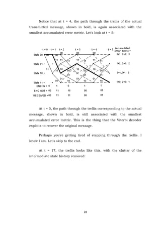
- 27. 27 equal, some people use a fair coin toss to choose the surviving predecessor state. Others simply pick one of them consistently, i.e. the upper branch or the lower branch. It probably doesn't matter which method you use. The operation of adding the previous accumulated error metrics to the new branch metrics, comparing the results, and selecting the smaller (smallest) accumulated error metric to be retained for the next time instant is called the add-compare-select operation. The figure below shows the results of processing t = 3: Note that the third channel symbol pair we received had a one- symbol error. The smallest accumulated error metric is a one, and there are two of these. Let's see what happens now at t = 4. The processing is the same as it was for t = 3. The results are shown in the figure:
- 28. 28 Notice that at t = 4, the path through the trellis of the actual transmitted message, shown in bold, is again associated with the smallest accumulated error metric. Let's look at t = 5: At t = 5, the path through the trellis corresponding to the actual message, shown in bold, is still associated with the smallest accumulated error metric. This is the thing that the Viterbi decoder exploits to recover the original message. Perhaps you're getting tired of stepping through the trellis. I know I am. Let's skip to the end. At t = 17, the trellis looks like this, with the clutter of the intermediate state history removed:
- 29. 29 The decoding process begins with building the accumulated error metric for some number of received channel symbol pairs, and the history of what states preceded the states at each time instant t with the smallest accumulated error metric. Once this information is built up, the Viterbi decoder is ready to recreate the sequence of bits that were input to the convolutional encoder when the message was encoded for transmission. This is accomplished by the following steps: First, select the state having the smallest accumulated error metric and save the state number of that state. Iteratively perform the following step until the beginning of the trellis is reached: Working backward through the state history table, for the selected state, select a new state which is listed in the state history table as being the predecessor to that state. Save the state number of each selected state. This step is called trace back. Now work forward through the list of selected states saved in the previous steps. Look up what input bit corresponds to a transition from each predecessor state to its successor state. That is the bit that must have been encoded by the convolutional encoder. The following table shows the accumulated metric for the full 15-bit (plus two flushing bits) example message at each time t:
- 30. 30 Table 2.4 Accumulated error metric for 15 bit message It is interesting to note that for this hard-decision-input Viterbi decoder example, the smallest accumulated error metric in the final state indicates how many channel symbol errors occurred. The following state history table shows the surviving predecessor states for each state at each time t: Table 2.5 surviving predecessor states for each state at each time t The following table shows the states selected when tracing the path back through the survivor state table shown above: Table 2.6 States selected when tracing the path back
- 31. 31 Using a table that maps state transitions to the inputs that caused them, we can now recreate the original message. Here is what this table looks like for our example rate 1/2 K = 3 convolutional code: Figure 2.7 State transition Maps to the inputs Note: In the above table, x denotes an impossible transition from one state to another state: So now we have all the tools required to recreate the original message from the message we received: Figure 2.8 Recreating the original message The two flushing bits are discarded. Here‟s an insight into how the traceback algorithm eventually finds its way onto the right path even if it started out choosing the wrong initial state. This could happen if more than one state had the smallest accumulated error metric, for example I‟ll use the figure for the trellis at t=3 again to illustrate this point:
- 32. 32 See how at t = 3, both States 012 and 112 had an accumulated error metric of 1. The correct path goes to State 012 -notice that the bold line showing the actual message path goes into this state. But suppose we choose State 112 to start our traceback. The predecessor state for State 112 , which is State 102 , is the same as the predecessor state for State 012! This is because at t = 2, State 102 had the smallest accumulated error metric. So after a false start, we are almost immediately back on the correct path. For the example 15-bit message, we built the trellis up for the entire message before starting traceback. For longer messages, or continuous data, this is neither practical nor desirable, due to memory constraints and decoder delay. Research has shown that a traceback depth of K x 5 is sufficient for Viterbi decoding with the type of codes we have been discussing. Any deeper traceback increases decoding delay and decoder memory requirements, while not significantly improving the performance of the decoder. The exception is punctured codes, which I'll describe later. They require deeper traceback to reach their final performance limits. To implement a Viterbi decoder in software, the first step is to build some data structures around which the decoder algorithm will be implemented. These data structures are best implemented as arrays. The primary six arrays that we need for the Viterbi decoder are as follows:
- 33. 33 A copy of the convolutional encoder next state table, the state transition table of the encoder. The dimensions of this table (rows x columns) are 2(K - 1) x 2k. This array needs to be initialized before starting the decoding process. A copy of the convolutional encoder output table. The dimensions of this table are 2(K - 1) x 2k. This array needs to be initialized before starting the decoding process. An array (table) showing for each convolutional encoder current state and next state, what input value (0 or 1) would produce the next state, given the current state. We'll call this array the input table. Its dimensions are 2(K - 1) x 2(K - 1). This array needs to be initialized before starting the decoding process. An array to store state predecessor history for each encoder state for up to K x 5 + 1 received channel symbol pairs. We'll call this table the state history table. The dimensions of this array are 2 (K - 1) x (K x 5 + 1). This array does not need to be initialized before starting the decoding process. An array to store the accumulated error metrics for each state computed using the add-compare-select operation. This array will be called the accumulated error metric array. The dimensions of this array are 2 (K - 1) x 2. This array does not need to be initialized before starting the decoding process. An array to store a list of states determined during traceback (term to be explained below). It is called the state sequence array. The dimensions of this array are (K x 5) + 1. This array does not need to be initialized before starting the decoding process. 2.7 CONCLUSION This chapter describes the detailed description of viterbi algorithm which is based on coding theory
- 34. 34 CHAPTER 3 VITERBI DECODER 3.1 INTRODUCTION In this chapter the main concept of convolutional encoding and decoding of encoded data by the use of Viterbi algorithm and the different blocks of viterbi decder are discussed. Convolutional encoding with Viterbi decoding is a powerful method for forward error correction. It has been widely deployed in many wireless communication systems to improve the limited capacity of the communication channels. The Viterbi algorithm is the most extensively employed decoding algorithm for convolutional codes. The Viterbi algorithm develops as an asymptotically optimal decoding algorithm for convolutional codes. It is well suited to hardware decoder implementation. Viterbi decoding of convolutional codes found to be efficient and robust. Viterbi decoding is the best-known implementation of the maximum likely-hood decoding. Here we narrow the options systematically at each time tick. The Viterbi decoder examines an entire received sequence of a given length. The decoder computes a metric for each path and makes a decision based on this metric. All paths are followed until two paths converge on one node. Then the path with the higher metric is kept and the one with lower metric is discarded. The most common metric used is the Hamming distance metric.
- 35. 35 3.2 CONVOLUTIONAL ENCODER Figure 3.1 block diagram for convolutional encoder As shown in figure 3.1, it will represent the block diagram for convolutional encoder. Mainly for this encoder block we will give 1-bit input data, after doing encoding it will generates c1 and c2 are the two outputs. To calculate c1 it will do XOR operation in between input bit, F6, F5, F4 & F1 outputs. Where as to calculate c2 it will do XOR operation in between input bit, F5, F4, F2, F1 outputs. 3.3 DECODER This project presents a configurable 3-bit soft decision Viterbi decoder implementation that meets the requirements for WLAN and broadband applications. The programmable design supports a constraint length K=7 soft decision Viterbi decoder (SDVD) realization with a code rate (R) of 1/2. To assure a high throughput, an architecture incorporating 64 Add Compare Select (ACS) units operating in parallel has been selected. Further low power adaptive viterbi decoder is developed which used strongly connected trellis decoding.
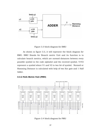
- 36. 36 To implement Viterbi algorithm in Reconfigurable Hardware like FPGA with the help of Hardware Descriptor Language, it‟s essential to translate algorithm in to digital Block. Algorithm demand computation of Path and Branch Metric and storage of Path Metric decision to Trace Back. Based on requirement Blocks are arranged as shown in figure 3.3 Figure 3.2 Block Diagram for Decoder 3.3.1 Branch Metric Unit(BMU) A branch metric unit's function is to calculate branch metrics, which are normed distances between every possible symbol in the code alphabet, and the received symbol. There are hard decision and soft decision Viterbi decoders. A hard decision Viterbi decoder receives a simple bit stream on its input, and a Hamming distance is used as a metric. A soft decision Viterbi decoder receives a bitstream containing information about the reliability of each received symbol. The squared Euclidean distance is used as a metric for soft decision decoders.
- 37. 37 Figure 3.3 block diagram for BMU As shown in figure 3.3, it will represent the block diagram for BMU. BMU Stands for Branch metric Unit and its function is to calculate branch metrics, which are normed distances between every possible symbol in the code alphabet and the received symbol. V1V2 represent a symbol where V1 and V2 is two bit of symbol. Normed or Hamming Distance is calculated with help of two Xor gate and 1 Half Adder. 3.3.2 Path Metric Unit (PMU) Figure 3.4 block diagram for PMU
- 38. 38 A path metric unit summarizes branch metrics to get metrics for 2K − 1 paths, one of which can eventually be chosen as optimal. Every clock it makes 2K − 1 decisions, throwing off wittingly nonoptimal paths. The results of these decisions are written to the memory of a traceback unit. In Path Metric Unit Eight Add Compare and Select Unit are arranged in particular fashion based on formation of Trelli‟s Diagram. Add Compare Select Unit Figure 3.5 block diagram for ACSU The core elements of a PMU are ACS (add-compare-select) units. The way in which they are connected between themselves is defined by a specific code‟s trellis diagram. Comparator After the computation of path metric, we have to find out the ACSU corresponding to we have maximum path metric. For this block mainly we will give the encoded output of 2-bit data. For the encoder block we gave in1 as a input in the sequence “0110001”. After decoding it has to give in the same sequence but in the reverse order i.e. we are getting as a decoded_ sequence output of 7-bit data. 3.3.3 Trace Back Unit(TBU) In the FPGA-based implementation, the memory for storing the survivor paths is divided into four memory banks, each of which
- 39. 39 stores 64 survivor paths. The trace back length of the design is chosen as D=8 that is equivalent to a trace back length of 8(K-1)=64 low- connectivity trellis stages. As mentioned earlier, this is large enough to ensure the convergence of the survivor paths. Since 2-D circular memory addressing scheme is used in this design, the size of each memory bank should be equal to 64X2-D=1024. and its word length 8 bits. The survivor path memory is organized as shown in Fig.3.6. Figure 3.6 Architecture of the trace back unit. There are three operation phases in the management of the memory, write new data (WR), trace back read (TB), and decode read (DR), which occupy memory with depths of D/2, D, and D/2, respectively. These three operations access the three logical blocks of the memory, respectively, by using 2-D circular memory addressing scheme , in which the trace back read and the decode read operations are performed by using one pointer instead of multiple ones. In view of the memory depths of WR, TB, and DR, it is noted that the read rate should be three times that of the write rate, so that the two read- phases and one write-phase can be performed simultaneously within the same time period. The write pointer advances forward from stage to stage in the trellis, and the decisions made by the ACS computations at all the trellis states regarding the survivors are written into the memory block that is just freed by the decode read operation. The read pointer traces back from stage to stage so that the RAM1024_0RAM1024_1RAM1024_2RAM1024_3BUS_MUXs5--s0s76 bits address for each RAM banks62/4 Decoder8 bit Shift register632 bit FILO registeren0en1Decoder outputen2en388888en0en1en2en3SurSurSurSur
- 40. 40 retrieved data after each read operation can be treated as a pointer to indicate the corresponding state number of the previous stage. When the decisions are written into the memory for one stage, the read pointer will trace back the memory by three stages. After D such trace backs, all the survivor paths will converge and the actual decoding takes place. There are D/2X8 = 32 bits of data decoded at each trace back iteration, and these retrieved data should be rearranged in its original order. The architecture of the trace back unit is shown in Fig.3.6. The four block select RAMs each of size of 1024X8 bits provided by the FPGA chip are used to implement the four memory banks, RAM1024_0 to RAM1024_3. At each stage, the survivor decisions made by the four pairs of the systolic arrays in Fig. 6 are written into the four corresponding memory banks. At each trace back read, the previously retrieved data (the state number) points to the current data to be read. The most significant two bits and , of the previously retrieved data in the register are sent to the 2/4 Decoder and BUS_MUX. These bits are used to select the memory bank to be accessed and to have its stored data retrieved. The least significant 6 bits , of the previously retrieved data in the register are used to address the 64 decisions in one of the memory banks selected at each read operation. In other words, at every trace back operation, one of the 64 decisions (corresponding to the 64 survivor paths) stored in the four memory banks can be read by using the previously retrieved data as a pointer. After D trace backs, corresponding to the eight strongly connected trellis stages, the decoded data is loaded into the 8-bit shift register and then shifted to the first-in-last-out (FILO) register. Finally, the decoded data is sent out in the reverse order from the FILO register. 3.4 CONCLUSION This chapter describes the basic viterbi decoder and uses the viterbi algorithm describe in chapter2.this gives basis for more complex viterbi decoders developed in next chapter.
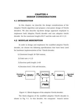
- 41. 41 CHAPTER 4 DESIGN CONSIDERATIONS 4.1 INTRODUCTION In this chapter, we describe the design considerations of the Adaptive Viterbi algorithm and propose a low-power design of Viterbi decoders. We also describe top-down design approach employed to implement both Adaptive Viterbi decoder and non adaptive viterbi decoder for the constraint length of K=7 and the code rate of r=1/2. 4.2 MODULAR MESCRIPTION In order to design and implement the modified adaptive Viterbi decoder, we choose the following specifications that have been used for hardware implementation of the Viterbi decoder: 1) Constraint length: K=7(64 states); 2) Code rate: r=1/2 3) Survivor path length: L=64 4) Decision level: 3-bit soft decision. Figure 4.1 Block diagram of the adaptive Viterbi decoder. The block diagram of the modified adaptive Viterbi decoder is shown in Fig. 4.1. In this decoder, the composite branch metric
- 42. 42 generation(CBM) unit is designed to collect the two soft input sequences and to compute all the possible branch metrics corresponding to the eight low-connectivity trellis stages. The path metric update unit is designed to generate the composite branch metrics and to process the matrix–vector ACS computation. The trace back unit can retrieve the decoded sequence from the survivor path memory through a trace back strategy. Figure 4.2 input buffer for the two soft inputs 4.3 COMPOSITE BRANCH METRIC UNIT 4.3.l Logic Diagram
- 43. 43 Figure 4.3 Unit to compute the eight one-stage branch metrics corresponding to a composite branch metric. The input buffer is designed to gather the two soft input sequences corresponding to a given strongly connected trellis stage so that the composite branch metrics of the stage can be generated. As shown in Fig. 5.1, the two soft inputs are sent to the corresponding 3- bit registers depending on the enable signal generated by the 3/8 decoder. The 3/8 decoder outputs the eight enable signals in a circular way so that the two soft input sequences corresponding to a strongly connected trellis stage are loaded into the 3-bit registers. The sequences are then buffered into two 24-bit registers and used to compute the corresponding eight one-stage branch metrics. Each of the eight one-stage branch metrics has four possible results depending on the corresponding two-bit codeword in the original low connectivity trellis stage. Table I gives the expressions for the evaluation of a one-stage branch metric under the four possible values of the two-bit codeword, where in1 and in2 represent the two soft inputs at the low-connectivity trellis stage. The eight one-stage branch metrics corresponding to a composite branch metric are computed by the unit shown in Fig.4.2, in which each one-stage branch metric is computed under the four possible values of the two-bit codeword, and is output to the array processors in BM_4s shown in Fig. 4.3. 4.3.2 Source Code Description In this module Composite one stage branch metrics are calculated combining 8 one stage branch metrics corresponding to a one stage branch metric.the inputs a,b,reset are applied to to one stage branch metricsto generate 9 bit BMU out put.
- 44. 44 4.4 ADD-COMPARE-SELECT 4.4.1 Logic Diagram Figure 4.4Arithmetic pipelined processor for ACS-4 The arithmetic-pipelining processor for an ACS_4 is shown in Fig.5.7. This processor is implemented with two pipeline stages. The adder in the first pipeline stage is used to compute the 64 path metrics at any of the corresponding 16 states of a given stage, whereas the adder in the second pipeline stage is used to make comparisons amongst the 64 path metrics computed by the first pipeline stage. The length of the adders including a sign bit in the two pipeline stages should be 10 bits in order to perform the modulo arithmetic. In the second pipeline stage, the comparison between the path metrics computed at the current and previous clock cycles at a state of a given stage are carried out by adding the path metric at the current clock cycle to the compliment of the path metric at the previous clock cycle, increased by unity. In this way, the sign-bit of the adder can represent the result of the comparison between the two path metrics. If the sign-bit is “1,” the path metric at the current clock cycle is smaller than the path metric at the previous clock cycle, and if the sign-bit is “0,” then the former is larger than the latter. In the 88881010101010Composite branch metricPath metricPath metricDecision bits (or Sur) AdderAdderRegRegRegRegCounter mux1mux2 Enable0011signCLK
- 45. 45 meantime, the path metric with the smaller metric at the state of a given stage is selected by the multiplexer (Mux1) and sent to the Register. In addition, the 8-bit counter in the second pipeline stage is used to represent the 64 possible states of the previous stage from which the paths originate and terminate at the various states of the present stage. One of these 64 paths would be the survivor path depending on the sign bit of the adder in the second pipeline stage, and is selected by the multiplexer (Mux2) at each clock cycle. Thus, at a given stage, the path metric and the survivor corresponding to any of the16 states can be updated through 64 clock cycles. It should be mentioned that the critical path of the design as determined from the Xilinx report is the second pipeline stage and consists of the 10-bit adder and the multiplexer. The synchronization between ACS_4 and BM_4 can be achieved by simply designing a timing scheme that makes them start at different time instants. This means that at a given stage the processors in an ACS_4 will not start their computations until the results from the processors in the corresponding BM_4 have been generated. In this way, throughput of the design will not be changed, but a latency between ACS_4 and BM_4 is introduced. This is in fact the latency of any processor in BM_4. Systolic Array Architecture Based Branch and Path metric Updating The modified adaptive Viterbi algorithm can be implemented using the systolic array architecture shown in Fig.5.8 in which time multiplexing, arithmetic pipelining are exploited. For K=7, the matrix vector ACS computation can be processed by 64×64 adjacency matrix Bq and the 1×64 path metric vector Pq-1.In this design ,the adjacency matrix Bq is partitioned in to four 64×16 sub matrices, and the four sub matrices along with the path metric vector Pq-1 are used to update the corresponding 64 path metrics of the given stage .This is achieved by the four pairs of interconnected systolic arrays is formed as shown
- 46. 46 in Fig 5.8,where the top interconnected four processors represent the systolic array BM-4 and the bottom interconnected four processors represent the systolic array ACS-4 . Figure 4.5 Architecture of a pair of systolic arrays. In the top systolic array the composite branch metric is generated by using equation (2) and (3).The code word vector C0j is divided in to four 1×64 sub vectors to be stored in four ROMs,ROM0 to ROM3and the code word Ci0 stored in the ROM. The codeword C0j stays inside each processor, and Ci0 moves to the right. In the bottom systolic array, the path metric Pq(j) of stage q is computed according to (10) and decisions on the survivor paths are made. The intermediate ACS result Rq(j) denoted by stays inside the j th processor, whereas Pq-1(j) of stage q-1 moves to the right. All data movements in the two systolic arrays are synchronized. This design can thus be viewed as a “result stay” systolic array architecture.
- 47. 47 Figure 4.6 Systolic array based architecture for adaptive viterbi decoder As shown in Fig. 4.7, for computing the corresponding four subsets of Bq at each stage, the codeword vector C0j is divided into four 1X 64 sub vectors to be stored in four ROMs, ROM0 to ROM3, and the codeword vector Ci0 stored in the ROM. Globally, the four sub matrix–vector ACS computations are carried out simultaneously by the corresponding four pairs of systolic arrays. Locally, inside each pair of the systolic arrays, the corresponding sub matrix–vector ACS computation is time multiplexed. For a given K the number of trellis states at a given stage is equal to 2K−1 . If the time-multiplexing technique is not employed, the number of pairs of systolic arrays (each array having 4 processors) is 2K−1/4 =2K−3 . For K=7 this is 64, BUS_MUXdm_plus_TMux1Mux2ROM0ROM1ROM2ROM3BM_4BM_4BM_4BM_4ACS_4ACS_4ACS_4ACS_4Mux_PMux_PMux_PMux_PMux_SMux_SMux_SMux_SSurSurSurSurCMPCMPCMPCMPRAM0RAM1RAM2RAM388888888101010101616161616161010101011111111111111111110101010ROMA pair of systolic arrays32YqSq-1(j) Pq-1(0),Pq-1(1),......,Pq-1(255) Sq-1(j)
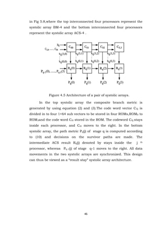
- 48. 48 and the total number of array processors is 512. As K increases, the number of array processors will increase exponentially, which is the same as in the case of the conventional butterfly architecture-based parallel Viterbi decoder. However, we employ a time-multiplexing technique. In this technique, when K=7, each pair of systolic arrays (each array having four processors) processes 64 out of 256 states sequentially in 16 iterations. For a given K , the more the number of systolic array pairs used, the fewer the number of iterations needed. Thus, as K increases, our time-multiplexing approach provides the flexibility to trade off the number of iterations with the number of systolic array pairs. 4.4.2Source code Description In this module the airthmatic pype line based Add compare select unit is developed.The two 9 bit inputs from BMU are given as input along with decode_in ,m,n,p,q,r,s,clk_sm,en,en_main,en2 and reset .This module generates 9 bit out puts which will be inputs for trace back operation. 4.5 TRACE BACK UNIT 4.5.1 Logic Diagram Figure 4.7 Architecture of the trace back unit. RAM1024_0 RAM1024_1 RAM1024_2 RAM1024_3 BUS_MUX s7 s5--s0 6 bits address for each RAM bank 2/4 Decoder s6 8 bit Shift register 6 32 bit FILO register en0 en1 Decoder output en2 en3 8 8 8 8 8 en0 en1 en2 en3 Sur Sur Sur Sur
- 49. 49 In the FPGA-based implementation, the memory for storing the survivor paths is divided into four memory banks, each of which stores 64 survivor paths. The trace back length of the design is chosen as D=8 that is equivalent to a trace back length of 8(K-1)=64 low- connectivity trellis stages. As mentioned earlier, this is large enough to ensure the convergence of the survivor paths. Since 2-D circular memory addressing scheme is used in this design, the size of each memory bank should be equal to 64X2-D=1024. and its word length 8 bits. The survivor path memory is organized as shown in Fig.4.8. There are three operation phases in the management of the memory, write new data (WR), trace back read (TB), and decode read (DR), which occupy memory with depths of D/2, D, and D/2, respectively. These three operations access the three logical blocks of the memory, respectively, by using 2-D circular memory addressing scheme , in which the trace back read and the decode read operations are performed by using one pointer instead of multiple ones. In view of the memory depths of WR, TB, and DR, it is noted that the read rate should be three times that of the write rate, so that the two read- phases and one write-phase can be performed simultaneously within the same time period. The write pointer advances forward from stage to stage in the trellis, and the decisions made by the ACS computations at all the trellis states regarding the survivors are written into the memory block that is just freed by the decode read operation. The read pointer traces back from stage to stage so that the retrieved data after each read operation can be treated as a pointer to indicate the corresponding state number of the previous stage. When the decisions are written into the memory for one stage, the read pointer will trace back the memory by three stages. After D such trace backs, all the survivor paths will converge and the actual decoding takes place. There are D/2X8 = 32 bits of data decoded at each trace back iteration, and these retrieved data should be rearranged in its original order
- 50. 50 The architecture of the trace back unit is shown in Fig.4.8. The four block select RAMs each of size of 1024X8 bits provided by the FPGA chip are used to implement the four memory banks, RAM1024_0 to RAM1024_3. At each stage, the survivor decisions made by the four pairs of the systolic arrays in Fig. 4.7 are written into the four corresponding memory banks. At each trace back read, the previously retrieved data (the state number) points to the current data to be read. The most significant two bits of the previously retrieved data in the register are sent to the 2/4 Decoder and BUS_MUX. These bits are used to select the memory bank to be accessed and to have its stored data retrieved. The least significant 6 bits , of the previously retrieved data in the register are used to address the 64 decisions in one of the memory banks selected at each read operation. In other words, at every trace back operation, one of the 64 decisions (corresponding to the 64 survivor paths) stored in the four memory banks can be read by using the previously retrieved data as a pointer. After D trace backs, corresponding to the eight strongly connected trellis stages, the decoded data is loaded into the 8-bit shift register and then shifted to the first-in-last-out (FILO) register. Finally, the decoded data is sent out in the reverse order from the FILO register. 4.5.2 Source code Description In this module The source code is developed based on the inputs from BMU and ACSU.This module retraces the Hamming distances.It links previously retrieved data in the register are used to address the 64 decisions in one of the memory banks selected at each read operation.
- 51. 51 4.6 ADAPTIVE VITERBI DECODER 4.6.1 Logic Diagram Figure 4.8 Block diagram of the adaptive Viterbi decoder. In this we are integrating all the sub modules i.e, CBMU , Systolic architecture of the AVA and the Trace Back Unit together to decode the encoded information shown in 5.11 for the constraint length K=7 and the code rate r=1/2. In this decoder the composite branch metric generation(CBM) unit is designed to collect the two soft input sequences and to compute all the possible branch metrics corresponding to the eight low-connectivity trellis stages. The path metric update unit is designed to generate the composite branch metrics and to process the matrix– vector ACS computation. The trace back unit can retrieve the decoded sequence from the survivor path memory through a trace back strategy. 4.6.2 Source code Description In this all the submodule codes are integrated as top module.The inputs are Decoder_in ,clk_sm,en and reset given as input to the top module and a 12 bit count_div_2_out ,onethird_clk_out,viterbi_out are generated giving aerror free decoded data.The convolutional decoder using adaptive Viterbi decoder is improvised version.
- 52. 52 4.7. CONCLUSION In this chapter the modular description of the three sub modules along with the Top order module are described elaborately.Based on this the source code implementation is taken up in next chapters.
- 53. 53 CHAPTER 5 SIMULATION RESULTS 5.1 INTRODUCTION This chapter focusses on the program flow description of each module. This chapter gives the simulation results of Encoder,Composte branch metric unit, add compare select unit, Survivor memory unit modules and Adaptive Viterbi Decoder (top order module). All these modules are synthesized using Xilinx ISE navigator tool. Simulations are usually divided in to following 5 categories. Behavioral simulation Functional simulation Gate level simulation or post synthesis simulation Switch level simulation Transistor-level or Circuit level simulation This is ordered from high-level to low-level simulation (high level being more abstract and low-level being more detailed). Proceeding from high-level to low-level, the simulation becomes more accurate, but they also become progressively more complex and take longer to run. While it is positive to perform a behavioral-level simulation of the whole system, it is just impossible to perform circuit-level simulation of more than few hundred transistors. Behavioral Simulation This method models large pieces of a system as black boxes withinput and outputs. This is done often using VHDL and Verilog. Functional Simulation This simulation ignores timing and includes delta-delay simulation, which sets the delays to a fixed value. Once a behavioral
- 54. 54 or functional simulation verifies the system working, the next step is to check the timing performance Logic Simulation or Gate-level simulation This simulation is used to check the timing performance of an ASIC. In the Gate-level simulation, a logic cell is treated as a black box modeled by a function whose variables are the input signals. The function may also model the delay through the logic cell setting all the delays to unit signals. The function may also model the delay through the logic cell. Setting all the delays to unit values is the equivalent of functional simulation. Switch-level Simulation This simulation can provide more accurate timing predictions than Gate-level simulation. Transistor-level Simulation These are the most accurate, but at the same time most complex and time-consuming simulation of all the simulations. This requires models of transistors, describing their nonlinear voltage and current characteristics. Simulation can also be divided on the basis of layout into two categories. Pre-layout Simulation Post-layout Simulation Simulation is used at many stages during the design. Initial Pre- layout Simulation includes logic-cell delays but no inter-connect delays. Estimates of capacitance may be included after completing logic synthesis, but only after physical design is over, Post-layout Simulation can be performed. In the Post-layout simulation, an SDF (Standard Delay Format) file is included in the simulation environment.
- 55. 55 5.2ENCODER 5.2.1 Simulation results Figure 5.1 Simulation results of Encoder 5.2.2 Signal Description S.No. Signal name Type Description 1. Clk Input triggers output 2. Data_in Input „1‟ bit stream 3. Reset Input Reset encoder 4. V2v1 Output Convolution output
- 56. 56 Port diagram Figure 5.2 port diagram of encoder 5.2.3 Logical description Mainly for this encoder block we will give 1-bit input data, after doing encoding it will generates V1 and V2 are the two outputs. To calculate V1 it will do XOR operation in between input bit, F6, F5, F4 & F1 outputs. Where as to calculate V2 it will do XOR operation in between input bit, F5, F4, F2, F1 outputs. As shown in figure 5.2, it will represent the simulation result for Convolutional encoder. Depending upon input i.e.data_in, it will generates the output i.e. v2v1 of 6-bit data.
- 57. 57 5.3 COMPOSITE BRANCH METRIC UNIT 5.3.1Simulation Results Figure 5.3 simulation results of composite branch metric unit 5.3.2 Signal Description S.NO Signal Name Type Description 1. a Input Load 2- bit input data 2. b Input Load 2- bit input data 3. Reset Input Reset pin is used to restart the BMU 4. c Output Generates 9-bit data
- 58. 58 Port diagram Figure 5.4 port diagram of composite branch metric unit 5.3.3 Logical Description The two soft inputs are sent to the corresponding 3-bit registers depending on the enable signal generated by the 3/8 decoder. The 3/8 decoder outputs the eight enable signals in a circular way so that the two soft input sequences corresponding to a strongly connected trellis stage are loaded into the 3-bit registers. 5.4 ADD COMPARE SELECT UNIT 5.4.1Simulation Results 5.5 Simulation result of Add compare select Unit
- 59. 59 5.4.2 Signal Description S.NO Signal Name Type Description 1. decoder_in Input Load 2- bit input data say „11‟ 2. m Input Load 2- bit input data „00‟ 3. n Input Reset pin is used to restart the BMU 4. p Input Load 2-bit data say „01‟ 5. q Input Load 2 bit input data say „00‟ 6. r Input Load 9 bit input data from BMU 7. s Input Load 9 bit input data from BMU 8. clk_sm Input If clk_sum =‟1‟ then ACS process sstarts 9. en Input en input „1‟ 10. en_main Input En_main input „1‟ 11. en2 Input 2nd enable 12. reset Input For resetting ACSU 13. x output 9 bitOutput for TBU 14. y output 9 bit output for TBU 15. e output Inputs for TBU 16. f output Input for TBU
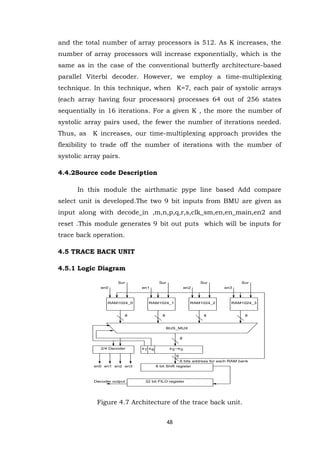
- 60. 60 Port diagram Figure 5.6 port diagram of ACSU 5.4.3 Logical Description The length of the adders including a sign bit in the two pipeline stages should be 10 bits in order to perform the modulo arithmetic. In the second pipeline stage, the comparison between the path metrics computed at the current and previous clock cycles at a state of a given stage are carried out by adding the path metric at the current clock cycle to the compliment of the path metric at the previous clock cycle, increased by unity.
- 61. 61 5.5 TRACE BACK UNIT 5.5.1Simulation results Figure 5.7 Simulation Result of Trace Back Unit. 5.5.2 Signal description The Trace back operation is having 64 Survivor memory paths and is having large no. of signals. 5.5.3 Logical Description The memory for storing the survivor paths is divided into four memory banks, each of which stores 64 survivor paths. The trace back length of the design is chosen as D=8 that is equivalent to a trace back length of 8(K-1)=64 low-connectivity trellis stages. 5.6 VITERBI DECODER In this we are integrating the all the sub modules ie CBMU , Systolic architecture of the AVA and the Trace Back Unit together to decode the encoded information shown in 5.11 for the constraint length K=7 and the code rate r=1/2.The simulation results are as follows.
- 62. 62 5.6.1 Simulation Results Figure 5.8 Simulation Result of complete Adaptive Viterbi Decoder 5.6.2 Signal Description S.No. SignalName Type Description 1. Decoder_in Input Convolutional Input 2. Clkk_sm Input Clock for triggering 3 En Input Enables viterbi decoder 4 Reset Input For resetting decoder 5 Count_div_2_out output 11 bit decoder output 6 Onethird_clk_out Output Clock reduction 7 Viterbi_out Output Viterbi output 5.6.3 Logical explanation In this decoder, the composite branch metric generation(CBM) unit is designed to collect the two soft input sequences and to compute all the possible branch metrics corresponding to the eight low-
- 63. 63 connectivity trellis stages. The path metric update unit is designed to generate the composite branch metrics and to process the matrix– vector ACS computation. The trace back unit can retrieve the decoded sequence from the survivor path memory through a trace back strategy. 5.7 CONCLUSION The focus of work in the low-power design of Viterbi decoders at logic level is reduction of dynamic power dissipation in the standard cell design environment. We considered two methods in this low power design , strongly connected trellis decoding and systolic array processing, in our design. These methods were applied to the survivor path storage block to reduce the number of ACS computations. The design flow that was followed is similar to the one used in industry. The behavior of a Viterbi decoder is described in VHDL. Then the design is synthesized to generate a gate level circuit in VERTEX II xc2vp30-7-ff896 as a target device in xilinx tool.
- 64. 64 CHAPTER 6 FPGA IMPLEMENTATION 6.1 INTRODUCTION This chapter describes the FPGA implementation of the proposed work using hardware description languages .This includes the pop module Viterbi decoder synthesis It describes the RTL views,port diagram,timing analysis chip vie floor plan etc.. of the implemented work. 6.2 SYNTHESIS REPORT Figure 6.1 Synthesis report of Viterbi decode
- 65. 65 HDL Synthesis Report of Adaptive Vitebi Decoder in VERTEX II xc2vp30-7-ff896 Macro statistics # RAMs : 4 1024x8-bit single-port RAM : 4 # Adders/Subtractors : 161 10-bit adder : 48 11-bit adder : 1 4-bit adder carry out : 16 5-bit adder : 16 5-bit adder carry out : 16 6-bit adder : 16 6-bit adder carry out : 16 7-bit adder : 16 7-bit adder carry out : 16 # Counters : 16 8-bit up counter : 16 # Registers : 529 1-bit register : 16 10-bit register : 17 11-bit register : 1 16-bit register : 6
- 66. 66 4-bit register : 336 5-bit register : 32 6-bit register : 32 7-bit register : 32 8-bit register : 57 # Latches : 1 4-bit latch : 1 # Multiplexers : 138 10-bit 4-to-1 multiplexer : 4 11-bit 4-to-1 multiplexer : 1 4-bit 4-to-1 multiplexer : 128 8-bit 4-to-1 multiplexer : 5 # Xors : 4 16-bit xor2 : 4 ========================================================= ================ * Final Report * ========================================================= ================ Final Results RTL Top Level Output File Name : viterbi_full.ngr Top Level Output File Name : viterbi_full
- 67. 67 Output Format : NGC Optimization Goal : Speed Keep Hierarchy : NO Design Statistics # IOs : 19 Cell Usage : # BELS : 7147 # BUF : 9 # GND : 1 # INV : 4 # LUT1 : 779 # LUT2 : 1799 # LUT2_D : 1 # LUT3 : 812 # LUT3_L : 6 # LUT4 : 993 # LUT4_D : 14 # MUXCY : 1627 # MUXF5 : 110 # MUXF6 : 48 # MUXF7 : 24
- 68. 68 # MUXF8 : 12 # VCC : 1 # XORCY : 907 # FlipFlops/Latches : 2854 # FDCE : 2461 # FDE : 384 # FDPE : 1 # FDPE_1 : 1 # LD : 6 # LDCE_1 : 1 # RAMS : 384 # RAM32X1S : 384 # Clock Buffers : 1 # BUFGP : 1 # IO Buffers : 18 # IBUF : 4 # OBUF : 14 ========================================================= ================
- 69. 69 Device utilization summary: --------------------------- Selected Device : 2vp30ff896-7 Number of Slices: 2778 out of 13696 20% Number of Slice Flip Flops: 2854 out of 27392 10% Number of 4 input LUTs: 5176 out of 27392 18% Number used as logic: 4408 Number used as RAMs: 768 Number of IOs: 19 Number of bonded IOBs: 19 out of 556 3% Number of GCLKs: 1 out of 16 6% Observation /comments Synthesis report gives the Gate level net list from a model described in VHDL. This gives the total information about the top module Viterbi Decoder in the form of number of logic gates, tri state buffers, number of Flip-Flops used and total number of registers..It is synthesized using Xilinx ISE navigator tool. The device utilized is xc2vp30-7-ff896.
- 70. 70 6.3 RTL VIEW The RTL view of Viterbi decoder is shown below. Figure 6.2 RTL Schematic of Adaptive Viterbi Decoder The RTL view gives a detailed account of the no.of Registers, Multiplexors, Buffers, etc.. in the implementation.The adaptive Viterbi decoder takes a little more area over Non adaptive viterbi decoder.But better performance in Power and lesser delay.
- 71. 71 6.4 PORT DIAGRAM Figure 6.3 Port diagram of Viterbi Decoder Port diagram explains the over all input output concept clearly. It describes How a convolutionally encoded input passing thro the Viterbi decoder gives error free reproduction of out put. 6.5 TIMING ANALYSYS Timing Summary: --------------- Speed Grade: -7 Minimum period: 5.176ns (Maximum Frequency: 193.192MHz) Minimum input arrival time before clock: 6.206ns Maximum output required time after clock: 3.514ns Maximum combinational path delay: No path found
- 72. 72 6.6 FLOOR PLAN Figure 6.4 Floor plan of Viterbi decoder Floor plan gives a lay out on the IC.Gives a clear idea about area of utilization of the device.
- 73. 73 6.7 CHIP VIEW Figure 6.5 Chip view of Viterbi decoder Chip view Gives idea of gives idea about the Chip a lay out description and before making final ASIC this helps.
- 74. 74 6.8 POWER DATA Figure 6.6 power data of viterbi Decoder Power data gives the final description of power calculation.In our implementation 28.1mw power is consumed. We measured the dynamic power dissipation of a circuit based on the switching activity from gate level simulation. Static power dissipation for cells is not considered for the measurement. This method is a compromise between power and area, and it is sufficient for our purpose.
- 75. 75 6.9 CONCLUSION Comparison of Synthesis Results Parameter Adaptive Viterbi Decoder Non Adaptive Viterbi Decoder Power 28.1 mw 103 mw Delay 1.13 nSec 2.71 nSec Area(No.Of IOBS) 223 205 Comparision of Synthesis Results. The design flow that was followed is similar to the one used in industry. The behavior of a Viterbi decoder is described in VHDL. Then the design is synthesized to generate a gate level circuit in VERTEX II xc2vp30-7-ff896 as a target device in xilinx tool.
- 76. 76 CHAPTER 7 CONCLUSION AND FUTURE SCOPE OF WORK 7.1 CONCLUSION -Convolutional coding is a coding scheme often employed in deep space communications and recently in digital wireless communications. -Viterbi decoders are used to decode convolutional codes. Viterbi decoders employed in digital wireless communications are complex in its implementation and dissipate large power. We proposed a Viterbi decoder design for low-power dissipation in this work. -The focus of work in the low-power design of Viterbi decoders at logic level is reduction of dynamic power dissipation in the standard cell design environment. - We considered two methods in this low power design , strongly connected trellis decoding and systolic array processing, in our design. These methods were applied to the survivor path storage block to reduce the number of ACS computations. -The design flow that was followed is similar to the one used in industry. The behavior of a Viterbi decoder is described in VHDL. Then the design is synthesized to generate a gate level circuit in VERTEX II xc2vp30-7-ff896 as a target device in xilinx tool. -We measured the dynamic power dissipation of a circuit based on the switching activity from gate level simulation. Static power dissipation for cells is not considered for the measurement. This method is a compromise between power and area, and it is sufficient for our purpose. - The systolic array processing with strongly connected trellis for adaptive viterbi decoder dissipates 28.1mW and has 1.13nSec of
- 77. 77 delay. The power saving is 66% compared with the non adaptive viterbi decoding with a less increase in area. -The data rates achievable can be very high compared to decoders of Constraint lenghths 3 or 4. 7.2 FUTURE SCOPE -As the VLSI technology is increasing rapidly in future the viterbi decoders with higher constraint lengths of 9 or 11 can be implemented for higher data rates.
- 78. 78 BIBLOGRAPHY 1. Abdul Rafeeq ,Abdul –shakoor and Valek Szwarc ”A High Performance soft decission viterbi decoder for WLAN and broand band application “IEEE Trans commun.,may 2006 2. F. Chan and D. Haccoun, “Adaptive Viterbi decoding of convolution codes over memory less channels,” IEEE Trans. Commun., vol. 45, no. 11, pp. 1389–1400, Nov. 1997. 3. C.-Y. Chang and K. Yao, “Systolic array processing of the Viterbi algorithm,” IEEE Trans. Inf. Theory, vol. 35, no. 1, pp. 76–86, Jan. 1989. 4. Y.-N. Chang, H. Suzuki, and K. K. Parhi,“A 2-Mb/s 256-state10- mw rate-1/3 Viterbi decoder,” IEEE J. Solid-State Circuits, vol. 35, no. 6, pp.826–834, Jun. 2000. . 5. Kang and A. N. Willson Jr., “Low-power Viterbi decoder for CDMA mobile terminals,” IEEE J. Solid-State Circuits, vol. 33, no. 3, pp.473– 482, Mar. 1998. 6. C.-Y. Chang and K. Yao, “Systolic array processing of the Viterbi algorithm,”IEEE Trans. Inf. Theory, vol. 35, no. 1, pp. 76–86, Jan. 1989. 7. C. G. Caraiscos and K. Z. Pekmestzi, “Low-latency bit-parallel systolic VLSI implementation of FIR digital filters,” IEEE Trans. Circuits Syst. II, Analog Digit. Signal Process., vol. 43, no. 7, pp. 529– 537, Jul. 1996. 8. S. Swaminathan, R. Tessier, D. Goeckel, and W. Burleson, “A dynamically reconfigurable adaptive Viterbi decoder,” in Proc. FPGA’02, 2002. 9. R. Henning and C. Chakrabarti, “Low-power approach for decoding
- 79. 79 convolutional codes with adaptive Viterbi algorithm approximations,” in Proc. ISLPED’02, Monterey, CA, Aug. 12–14, 200 2 Books: 1. “Digital Logic and Design” – Moris Mano, PHI Publications, 3rd Edition. 2. “VHDL Premier” – J. Bhaskar, 3rd Edition. 3. Douglas L.Perry, “VHDL programming by example”, fourth edition, TATA McGraw –Hill edition. 4. Charles H.Roth, Jr “Digital Design using VHDL”, Thamson Brooks/Cole. 5. Peter J.Ashenden “The Designers Guide to VHDL”, Second Edition, Morgan Kaufmanns Publishers, 2001. 6. “coding and decoding with convolutional codes” by charan Langton, editor. Websites: 1. www.wikipedia.com 2. www.xilinx.com 3. www.opencores.org 4. www. Complextoreal.com
- 80. 80 APPENDIX-A VLSI DESIGN FLOW INTRODUCTION The word digital has made a dramatic impact on our society. More significant is a continuous trend towards digital solutions in all areas – from electronic instrumentation, control, data manipulation, signals processing, telecommunications etc., to consumer electronics. Development of such solutions has been possible due to good digital system design and modelling techniques. CONVENTIONAL APPROACH TO DIGITAL DESIGN Digital ICs of SSI and MSI types have become universally standardized and have been accepted for use. Whenever a designer has to realize a digital function, he uses a standard set of ICs along with a minimal set of additional discrete circuitry. Consider a simple example of realizing a function as Q n+1 = Q n + (A B) Here On, A, and B are Boolean variables, with Q n being the value of Q at the nth time step. Here A B signifies the logical AND of A and B; the „+‟ symbol signifies the logical OR of the logic variables on either side. A circuit to realize the function is shown in Figure 1. The circuit can be realized in terms of two ICs – an A-O-I gate and a flip-flop. It can be directly wired up, tested, and used.
- 81. 81 A simple digital circuit With comparatively larger circuits, the task mostly reduces to one of identifying the set of ICs necessary for the job and interconnecting; rarely does one have to resort to a micro level design [Wakerly]. The accepted approach to digital design here is a mix of the top-down and bottom-up approaches as follows [Hill & Peterson]: • Decide the requirements at the system level and translate them to circuit requirements. • Identify the major functional blocks required like timer, DMA unit, register file etc., and say as in the design of a processor. • Whenever a function can be realized using a standard IC, use the same –for example programmable counter, mux, demux, etc. • Whenever the above is not possible, form the circuit to carry out the block functions using standard SSI – for example gates, flip-flops, etc. • Use additional components like transistor, diode, resistor, capacitor, etc., wherever essential. Once the above steps are gone through, a paper design is ready. Starting with the paper design, one has to do a circuit layout. The physical location of all the components is tentatively decided; they are interconnected and the „circuit-onpaper‟ is made ready. Once a paper design is done, a layout is carried out and a net-list prepared. Based
- 82. 82 on this, the PCB is fabricated and populated and all the populated cards tested and debugged. Sequence of steps in conventional electronic circuit design At the debugging stage one may encounter three types of problems: • Functional mismatch: The realized and expected functions are different. One may have to go through the relevant functional block carefully and locate any error logically. Finally the necessary correction has to be carried out in hardware. • Timing mismatch: The problem can manifest in different forms. One possibility is due to the signal going through different propagation delays in two paths and arriving at a point with a timing mismatch. This can cause faulty operation. Another possibility is a race condition in a circuit involving asynchronous feedback. This kind of problem may call for elaborate debugging. The preferred practice is to do debugging at smaller module stages and ensuring that feedback through larger loops is avoided: It becomes essential to check for the existence of long asynchronous loops.
- 83. 83 • Overload: Some signals may be overloaded to such an extent that the signal transition may be unduly delayed or even suppressed. The problem manifests as reflections and erratic behaviour in some cases (The signal has to be suitably buffered here.). In fact, overload on a signal can lead to timing mismatches. The above have to be carried out after completion of the prototype PCB manufacturing; it involves cost, time, and also a redesigning process to develop a bug free design. VLSI DESIGN The complexity of VLSI‟s being designed and used today makes the manual approach to design impractical. Design automation is the order of the day. With the rapid technological developments in the last two decades, the status of VLSI technology is characterized by the following [Wai-kai, Gopalan]: • A steady increase in the size and hence the functionality of the ICs. • A steady reduction in feature size and hence increase in the speed of operation as well as gate or transistor density. • A steady improvement in the predictability of circuit behaviour. • A steady increase in the variety and size of software tools for VLSI design. The above developments have resulted in a proliferation of approaches to VLSI design. We briefly describe the procedure of automated design flow [Rabaey, Smith MJ]. The aim is more to bring out the role of a Hardware Description Language (HDL) in the design process. An abstraction based model is the basis of the automated design.
- 84. 84 Abstraction Model The model divides the whole design cycle into various domains (see Figure 3). With such an abstraction through a division process the design is carried out in different layers. The designer at one layer can function without bothering about the layers above or below. The thick horizontal lines separating the layers in the figure signify the compartmentalization. As an example, let us consider design at the gate level. The circuit to be designed would be described in terms of truth tables and state tables. With these as available inputs, he has to express them as Boolean logic equations and realize them in terms of gates and flip-flops. In turn, these form the inputs to the layer immediately below. Compartmentalization of the approach to design in the manner described here is the essence of abstraction; it is the basis for development and use of CAD tools in VLSI design at various levels. The design methods at different levels use the respective aids such as Boolean equations, truth tables, state transition table, etc. But the aids play only a small role in the process. To complete a design, one may have to switch from one tool to another, raising the issues of tool compatibility and learning new environments. ASIC DESIGN FLOW As with any other technical activity, development of an ASIC starts with an idea and takes tangible shape through the stages of development as shown in Figure 4 and shown in detail in Figure 5. The first step in the process is to expand the idea in terms of behaviour of the target circuit. Through stages of programming, the same is fully developed into a design description – in terms of well defined standard constructs and conventions.
- 85. 85 Design domain and levels of abstraction Major activities in ASIC design The design is tested through a simulation process; it is to check, verify, and ensure that what is wanted is what is described. Simulation is carried out through dedicated tools. With every simulation run, the simulation results are studied to identify errors in the design description. The errors are corrected and another simulation run carried out. Simulation and changes to design
- 86. 86 description together form a cyclic iterative process, repeated until an error-free design is evolved. Design description is an activity independent of the target technology or manufacturer. It results in a description of the digital circuit. To translate it into a tangible circuit, one goes through the physical design process. The same constitutes a set of activities closely linked to the manufacturer and the target Technology. Design Description The design is carried out in stages. The process of transforming the idea into a detailed circuit description in terms of the elementary circuit components constitutes design description. The final circuit of such an IC can have up to a billion such components; it is arrived at in a step-by-step manner. The first step in evolving the design description is to describe the circuit in terms of its behaviour. The description looks like a program in a high level language like C. Once the behavioural level design description is ready, it is tested extensively with the help of a simulation tool; it checks and confirms that all the expected functions are carried out satisfactorily. If necessary, this behavioural level routine is edited, modified, and rerun – all done manually. Finally, one has a design for the expected system – described at the behavioural level. The behavioural design forms the input to the synthesis tools, for circuit synthesis. The behavioural constructs not supported by the synthesis tools are replaced by data flow and gate level constructs. To surmise, the designer has to develop synthesizable codes for his design.
- 87. 87 ASIC design and development flow The design at the behavioural level is to be elaborated in terms of known and acknowledged functional blocks. It forms the next detailed level of design description. Once again the design is to be tested through simulation and iteratively corrected for errors. The elaboration can be continued one or two steps further. It leads to a detailed design description in terms of logic gates and transistor switches.
- 88. 88 Optimization The circuit at the gate level – in terms of the gates and flip-flops – can be redundant in nature. The same can be minimized with the help of minimization tools. The step is not shown separately in the figure. The minimized logical design is converted to a circuit in terms of the switch level cells from standard libraries provided by the foundries. The cell based design generated by the tool is the last step in the logical design process; it forms the input to the first level of physical design [Micheli]. Simulation The design descriptions are tested for their functionality at every level – behavioural, data flow, and gate. One has to check here whether all the functions are carried out as expected and rectify them. All such activities are carried out by the simulation tool. The tool also has an editor to carry out any corrections to the source code. Simulation involves testing the design for all its functions, functional sequences, timing constraints, and specifications. Normally testing and simulation at all the levels – behavioural to switch level – are carried out by a single tool; the same is identified as “scope of simulation tool” in Figure 5. Synthesis With the availability of design at the gate (switch) level, the logical design is complete. The corresponding circuit hardware realization is carried out by a synthesis tool. Two common approaches are as follows: • The circuit is realized through an FPGA [Old field]. The gate level design description is the starting point for the synthesis here. The FPGA vendors provide an interface to the synthesis tool. Through the interface the gate level design is realized as a final circuit. With many synthesis tools, one can directly use the design description at the data
- 89. 89 flow level itself to realize the final circuit through an FPGA. The FPGA route is attractive for limited volume production or a fast development cycle. • The circuit is realized as an ASIC. A typical ASIC vendor will have his own library of basic components like elementary gates and flip- flops. Eventually the circuit is to be realized by selecting such components and interconnecting them conforming to the required design. This constitutes the physical design. Being an elaborate and costly process, a physical design may call for an intermediate functional verification through the FPGA route. The circuit realized through the FPGA is tested as a prototype. It provides another opportunity for testing the design closer to the final circuit. Physical Design A fully tested and error-free design at the switch level can be the starting point for a physical design [Baker & Boyce, Wolf]. It is to be realized as the final circuit using (typically) a million components in the foundry‟s library. The step-by-step activities in the process are described briefly as follows: • System partitioning: The design is partitioned into convenient compartments or functional blocks. Often it would have been done at an earlier stage itself and the software design prepared in terms of such blocks. Interconnection of the blocks is part of the partition process. • Floor planning: The positions of the partitioned blocks are planned and the blocks are arranged accordingly. The procedure is analogous to the planning and arrangement of domestic furniture in a residence. Blocks with I/O pins are kept close to the periphery; those which interact frequently or through a large number of interconnections are kept close together, and so on. Partitioning and floor planning may have to be carried out and refined iteratively to yield best results.
- 90. 90 • Placement: The selected components from the ASIC library are placed in position on the “Silicon floor.” It is done with each of the blocks above. • Routing: The components placed as described above are to be interconnected to the rest of the block: It is done with each of the blocks by suitably routing the interconnects. Once the routing is complete, the physical design cam is taken as complete. The final mask for the design can be made at this stage and the ASIC manufactured in the foundry. Post Layout Simulation Once the placement and routing are completed, the performance specifications like silicon area, power consumed, path delays, etc., can be computed. Equivalent circuit can be extracted at the component level and performance analysis carried out. This constitutes the final stage called “verification.” One may have to go through the placement and routing activity once again to improve performance. Critical Subsystems The design may have critical subsystems. Their performance may be crucial to the overall performance; in other words, to improve the system performance substantially, one may have to design such subsystems afresh. The design here may imply redefinition of the basic feature size of the component, component design, placement of components, or routing done separately and specifically for the subsystem. A set of masks used in the foundry may have to be done afresh for the purpose. ROLE OF HDL An HDL provides the framework for the complete logical design of the ASIC. All the activities coming under the purview of an HDL are shown enclosed in bold dotted lines in Figure 1.4. Verilog and VHDL are the two most commonly used HDLs today. Both have constructs
- 91. 91 with which the design can be fully described at all the levels. There are additional constructs available to facilitate setting up of the test bench, spelling out test vectors for them and “observing” the outputs from the designed unit. IEEE has brought out Standards for the HDLs, and the software tools conform to them. Verilog as an HDL was introduced by Cadence Design Systems; they placed it into the public domain in 1990. It was established as a formal IEEE Standard in 1995. The revised version has been brought out in 2001. However, most of the simulation tools available today conform only to the 1995 version of the standard. VHDL used by a substantial number of the VLSI designers today is the used in this project for modelling the design.