GENERIC SYSTEM VERILOG UNIVERSAL VERIFICATION METHODOLOGY BASED REUSABLE VERIFICATION ENVIRONMENT FOR EFFICIENT VERIFICATION OF IMAGE SIGNAL PROCESSING IPS/SOCS
0 likes22 views

The document presents an ultra-low power robust Kogge-Stone adder designed for implantable biomedical devices that operate at sub-threshold voltages to enhance battery life. Significant improvements in performance are achieved using forward body biasing and multi-threshold transistor techniques, aimed at reducing power delay products while maintaining operational efficiency. Simulations performed with a 45nm CMOS process demonstrate that the forward body biasing technique outperforms other methods in achieving energy savings and better performance metrics at low supply voltages.
![International Journal of VLSI design & Communication Systems (VLSICS) Vol.8, No.6, December 2017
DOI : 10.5121/vlsic.2017.8601 1
AN ULTRA-LOW POWER ROBUST KOGGE-
STONE ADDER AT SUB-THRESHOLD VOLTAGES
FOR IMPLANTABLE BIO-MEDICAL DEVICES
Sruthi Nanduru, Santosh Koppa and Eugene John
Department of Electrical and Computer Engineering
University of Texas at San Antonio, Texas, USA
ABSTRACT
The growing demand for energy constrained applications and portable devices have created a dire need for
ultra-low power circuits. Implantable biomedical devices such as pacemakers need ultra-low power
circuits for a better battery life for uninterrupted biomedical data processing. Circuits operating in sub-
threshold region minimize the energy per operation, thus providing a better platform for energy
constrained implantable biomedical devices. This paper presents 8, 16 and 32-bit ultra-low power robust
Kogge-Stone adders with improved performance. These adders operate at subthreshold supply voltages
which can be used for low power implantable bio-medical devices such as pacemakers. To improve the
performance of these adders in sub-threshold region, forward body bias technique and multi-threshold
transistors are used. The adders are designed using NCSU 45nm bulk CMOS process library and the
simulations were performed using HSPICE circuit simulator. Quantitative power-performance analysis is
performed at slow-slow (SS), typical-typical (TT) and fast-fast (FF) corners clocked at 50 KHz for
temperature ranging from 25̊C to 120̊C. For a supply voltage 0.3V, all the adders had the least PDP. Using
0.3V as the supply voltage, multi threshold voltage and forward body biasing techniques were applied to
further improve the performance of the adders. The PDP obtained using the forward body biasing
technique shows an effective improvement compared to high threshold voltage and multi threshold voltage
techniques. The forward biasing technique maintains a balance between delay reduction and increase in
average power, thus reducing the power delay product when compared to the other two techniques.
KEYWORDS
Kogge-Stone adder, Bio-Medical, Sub-Threshold, Forward body bias, Multi Threshold.
1. INTRODUCTION
The growing market for energy constrained applications and portable devices have created a dire
need for circuits operating at low supply voltages and consume less power. Many portable
biomedical devices require ultra-low power and improved battery life for uninterrupted
biomedical data processing. Low power systems need to operate at low voltages and/or low
currents. A recent explosion in applications that benefit from low energy operation has carved out
a significant niche for sub-threshold circuits. Digital circuits operating with a supply voltage less
than the threshold voltage of the transistors are said to be operating in the sub-threshold region.
Circuits operating in the sub-threshold region consume less active power and dissipate less
leakage power [1]. With the increased demand of the on-board processing of signals in the
implantable devices, designing circuits that consume low power and also perform complex real-
time signal processing is a challenging task. One of the complex signal processing tasks in](https://image.slidesharecdn.com/8617vlsi01-190404125137/85/GENERIC-SYSTEM-VERILOG-UNIVERSAL-VERIFICATION-METHODOLOGY-BASED-REUSABLE-VERIFICATION-ENVIRONMENT-FOR-EFFICIENT-VERIFICATION-OF-IMAGE-SIGNAL-PROCESSING-IPS-SOCS-1-320.jpg)
![International Journal of VLSI design & Communication Systems (VLSICS) Vol.8, No.6, December 2017
2
implantable devices such as pacemakers is the calculation of the Fast Fourier transform (FFT).
Basic building block of these FFTs are adders.
Addition is an indispensable operation in any digital, analog, or control system. An adder is one
of the critical components of a processor, as it can be used in the arithmetic logic units, floating-
point units and in the memory address generation unit. The fast and accurate operation of a digital
system mainly depends on the resident adders in the system. Among all the current adders,
parallel prefix adders are known to have better performance[2]. These parallel prefix adders are
known as carry tree adders.
The carry is generated parallelly in a tree adder and computation speed is improved at the cost of
increased area and power consumption. The main advantage of a carry tree design is that the
number of logic levels is reduced by generating the carries in parallel [2]. Due to the complexity
O (log_2 N) delay through the carry path, the parallel-prefix tree adders are better in terms of
speed. Kogge-Stone adder, Brent-Kung adder, Han-Carlson adder, and Sklansky adder are some
of the parallel prefix adders. Among all the parallel adders, Kogge-stone adder is the fastest
adder. This is due to the reduced number of stages needed to compute the sum and carry in the
Kogge-Stone adders. Kogge-Stone adder implementation is straightforward and also has one of
the shortest critical paths among all the tree adders [2].To utilize this adder for a low power
implantable device, it can be operated in subthreshold region [5]- [8]. In subthreshold region the
performance of the adders is degraded making it unsuitable for signal/data processing. In order to
improve the performance in subthreshold region, forward body bias (FBB) [9]- [12] and multi
threshold transistor (MVT) techniques [3]-[4] are used. This research conducts a quantitative
power-performance analysis of the Kogge-Stone adder using 45nm bulk CMOS technology in
typical-typical (TT), slow-slow (SS) and fast-fast (FF) corners at various operating temperatures.
The rest of this paper is organized as follows. Section 2 describes the steps involved in the
addition operation of the Kogge-Stone adder. Section 3 describes the tools and methodologies
used in simulating the Kogge-Stone adders. Section 4 discusses the simulation results and Section
5 concludes the paper.
2. THE KOGGE-STONE ADDER
The Kogge-Stone adder is a parallel prefix adder form of Carry Look Ahead (CLA) adder. The
Kogge-Stone adder requires more area to implement, but has less fan-out at each stage. In this
research, the Kogge-Stone adder is designed in the sub threshold region to reduce its power
consumption. The architecture of a Kogge-Stone adder is described below.
The functionality of the Kogge-Stone adder can be analysed through three distinct steps as shown
in Figure 1.
Figure 1: The three distinct stages of the Kogge-Stone Adder.](https://image.slidesharecdn.com/8617vlsi01-190404125137/85/GENERIC-SYSTEM-VERILOG-UNIVERSAL-VERIFICATION-METHODOLOGY-BASED-REUSABLE-VERIFICATION-ENVIRONMENT-FOR-EFFICIENT-VERIFICATION-OF-IMAGE-SIGNAL-PROCESSING-IPS-SOCS-2-320.jpg)
![International Journal of VLSI design & Communication Systems (VLSICS) Vol.8, No.6, December 2017
3
Figure 2 shows the schematic block diagram of an 8-bit Kogge-Stone adder. It consists of 3 carry
look-ahead network stages. The n-bit Kogge-Stone adder consists of log2n carry look ahead
network stages [13]. Hence, the 16-bit and 32-bit Kogge-Stone adder consists of 4 and 5 carry
look-ahead network stages, respectively.
Figure 2: The Schematic block diagram of an 8-Bit Kogge-Stone Adder.
Pre-Processing stage:In the pre-processing step, propagate and generate signals are computed
corresponding to each pair of A and B bitsas givenby Equations (1) and (2).
G = Ai AND Bi (1)
P = Ai XOR Bi (2)
Carry Generation Network:
In this stage, the carries are computed. All the operations are executed in parallel. They are
segmented after the computation of the carry. It uses carry propagate and generate which are
given by the logic Equations (3) and (4).
G = Gi OR (Pi AND G(iprev )) (3)
P=Pi AND P(iprev )
(4)
Post Processing:This step involves the computation of sum bits and final carry given by
Equations (5) and (6).
Ci = Gi (5)
Si = Pi XOR C(iprev ) (6)](https://image.slidesharecdn.com/8617vlsi01-190404125137/85/GENERIC-SYSTEM-VERILOG-UNIVERSAL-VERIFICATION-METHODOLOGY-BASED-REUSABLE-VERIFICATION-ENVIRONMENT-FOR-EFFICIENT-VERIFICATION-OF-IMAGE-SIGNAL-PROCESSING-IPS-SOCS-3-320.jpg)


![International Journal of VLSI design & Communication Systems (VLSICS) Vol.8, No.6, December 2017
12
obtained using MVT was at least twice that of the PDP obtained using the FBB technique for all
the adders.
REFERENCES
[1] Alice Wang , Benton Highsmith Calhoun , Chandrakasan. “Sub-threshold Design for Ultra-Low
Power Systems”, Integrated Circuits and Systems, 2006th Edition.
[2] Priya Gupta, Anu Gupta and Abhijit Asati, “Power-Aware Design of Logarithmic Prefix Adders in
Sub-threshold Regime: A comparative Analysis”, International Conference on Information and
Communication Technologies, 2015, pp. 1401-1408.
[3] T. McPherson et al., “760 MHz G6 S/390 Microprocessor Exploiting Multiple V_t and Copper
Interconnects,” Proceedings of the IEEE International Solid-State Circuits Conference, pp. 96-97,
February 2000.
[4] J.T. Kao and A. Chandrakasan, “Dual-Threshold Voltage Techniques for Low Power Digital
Circuits,” IEEE Journal of Solid-State Circuits, Vol. 35, No. 7, pp. 1009-1018, July 2000.
[5] A. Raychowdhury, B. C. Paul, S. Bhunia, and K. Roy, “Computing with sub-threshold leakage:
Device/circuit/architecture co-design for ultralow power sub-threshold operation”, IEEE Trans. Very
Large Scale Integr. (VLSI) Syst., vol. 13, no. 11, pp. 1213–1224, Nov. 2005.
[6] J. P. Campbell, L. C. Yu, K. P. Cheung, J. Qin, J. S. Suehle, A. Oates, and K. Sheng, “Large random
telegraph noise in sub-threshold operation of nano-scale n MOSFETs”, in Proc. IEEE Int. Conf. IC
Design Technol., May 2009, pp. 17–20.
[7] Priya Gupta, Anu Gupta and Abhijit Asati, “A Review on Ultra Low Power Design Technique:
Subthreshold Logic”, International Journal of Computer Science and Technology, April-June 2013,
pp. 64-71.
[8] D.Bol, R.Ambroise, D.Flandre and J.D.Legat. “Interests and limitations of technology scaling for
subthreshold logic,” IEEE Transactions on Very Large Scale Integration (VLSI) Systems, vol. 17, no.
10, pp. 1508–1519, 2009.
[9] S. Narendra, D. Antoniadis, and V. De, “Impact of Using Adaptive Body Bias to Compensate Die-to-
Die V_t Variation on Within-die V_t variation,” Proceedings of the IEEE International Symposium
on Low Power Electronics and Design, pp. 229-232, August 1999.
[10] A. Keshavarzi et al., “Technology Scaling Behavior of Optimum Reverse Body Bias for Standby
Leakage Power Reduction in CMOS IC’s,” Proceedings of the IEEE International Symposium on
Low Power Electronics and Design, pp. 252-254, July 1999.
[11] C. Wann et al., “CMOS with Active Well Bias for Low Power and RF/Analog Applications,”
Proceedings of the IEEE International Symposium on VLSI Technology, pp. 158-159, June 2000.
[12] S. –F. Huang et al., “Scalability and Biasing Strategy for CMOS with Active Well Bias,” Proceedings
of the IEEE International Symposium on VLSI Technology, pp. 107-108, June 2001.
[13] Raghav, Himadri Singh, Sachin Maheswari, and B. Prasad Singh. "Performance Analysis of
Subthreshold 32-Bit Kogge-Stone Adder for Worst-Case-Delay and Power in Sub-micron
Technology." Communications in Computer and Information Science VLSI Design and Test (2013):
100-07.
[14] Gupta, S. K., A. Raychowdhury and K. Roy. "Digital Computation in Subthreshold Region for
Ultralow-Power Operation: A Device-Circuit-Architecture Codesign Perspective." Proceedings of the
IEEE 98, no. 2 (2010): 160-190.](https://image.slidesharecdn.com/8617vlsi01-190404125137/85/GENERIC-SYSTEM-VERILOG-UNIVERSAL-VERIFICATION-METHODOLOGY-BASED-REUSABLE-VERIFICATION-ENVIRONMENT-FOR-EFFICIENT-VERIFICATION-OF-IMAGE-SIGNAL-PROCESSING-IPS-SOCS-12-320.jpg)

GENERIC SYSTEM VERILOG UNIVERSAL VERIFICATION METHODOLOGY BASED REUSABLE VERIFICATION ENVIRONMENT FOR EFFICIENT VERIFICATION OF IMAGE SIGNAL PROCESSING IPS/SOCS
- 1. International Journal of VLSI design & Communication Systems (VLSICS) Vol.8, No.6, December 2017 DOI : 10.5121/vlsic.2017.8601 1 AN ULTRA-LOW POWER ROBUST KOGGE- STONE ADDER AT SUB-THRESHOLD VOLTAGES FOR IMPLANTABLE BIO-MEDICAL DEVICES Sruthi Nanduru, Santosh Koppa and Eugene John Department of Electrical and Computer Engineering University of Texas at San Antonio, Texas, USA ABSTRACT The growing demand for energy constrained applications and portable devices have created a dire need for ultra-low power circuits. Implantable biomedical devices such as pacemakers need ultra-low power circuits for a better battery life for uninterrupted biomedical data processing. Circuits operating in sub- threshold region minimize the energy per operation, thus providing a better platform for energy constrained implantable biomedical devices. This paper presents 8, 16 and 32-bit ultra-low power robust Kogge-Stone adders with improved performance. These adders operate at subthreshold supply voltages which can be used for low power implantable bio-medical devices such as pacemakers. To improve the performance of these adders in sub-threshold region, forward body bias technique and multi-threshold transistors are used. The adders are designed using NCSU 45nm bulk CMOS process library and the simulations were performed using HSPICE circuit simulator. Quantitative power-performance analysis is performed at slow-slow (SS), typical-typical (TT) and fast-fast (FF) corners clocked at 50 KHz for temperature ranging from 25̊C to 120̊C. For a supply voltage 0.3V, all the adders had the least PDP. Using 0.3V as the supply voltage, multi threshold voltage and forward body biasing techniques were applied to further improve the performance of the adders. The PDP obtained using the forward body biasing technique shows an effective improvement compared to high threshold voltage and multi threshold voltage techniques. The forward biasing technique maintains a balance between delay reduction and increase in average power, thus reducing the power delay product when compared to the other two techniques. KEYWORDS Kogge-Stone adder, Bio-Medical, Sub-Threshold, Forward body bias, Multi Threshold. 1. INTRODUCTION The growing market for energy constrained applications and portable devices have created a dire need for circuits operating at low supply voltages and consume less power. Many portable biomedical devices require ultra-low power and improved battery life for uninterrupted biomedical data processing. Low power systems need to operate at low voltages and/or low currents. A recent explosion in applications that benefit from low energy operation has carved out a significant niche for sub-threshold circuits. Digital circuits operating with a supply voltage less than the threshold voltage of the transistors are said to be operating in the sub-threshold region. Circuits operating in the sub-threshold region consume less active power and dissipate less leakage power [1]. With the increased demand of the on-board processing of signals in the implantable devices, designing circuits that consume low power and also perform complex real- time signal processing is a challenging task. One of the complex signal processing tasks in
- 2. International Journal of VLSI design & Communication Systems (VLSICS) Vol.8, No.6, December 2017 2 implantable devices such as pacemakers is the calculation of the Fast Fourier transform (FFT). Basic building block of these FFTs are adders. Addition is an indispensable operation in any digital, analog, or control system. An adder is one of the critical components of a processor, as it can be used in the arithmetic logic units, floating- point units and in the memory address generation unit. The fast and accurate operation of a digital system mainly depends on the resident adders in the system. Among all the current adders, parallel prefix adders are known to have better performance[2]. These parallel prefix adders are known as carry tree adders. The carry is generated parallelly in a tree adder and computation speed is improved at the cost of increased area and power consumption. The main advantage of a carry tree design is that the number of logic levels is reduced by generating the carries in parallel [2]. Due to the complexity O (log_2 N) delay through the carry path, the parallel-prefix tree adders are better in terms of speed. Kogge-Stone adder, Brent-Kung adder, Han-Carlson adder, and Sklansky adder are some of the parallel prefix adders. Among all the parallel adders, Kogge-stone adder is the fastest adder. This is due to the reduced number of stages needed to compute the sum and carry in the Kogge-Stone adders. Kogge-Stone adder implementation is straightforward and also has one of the shortest critical paths among all the tree adders [2].To utilize this adder for a low power implantable device, it can be operated in subthreshold region [5]- [8]. In subthreshold region the performance of the adders is degraded making it unsuitable for signal/data processing. In order to improve the performance in subthreshold region, forward body bias (FBB) [9]- [12] and multi threshold transistor (MVT) techniques [3]-[4] are used. This research conducts a quantitative power-performance analysis of the Kogge-Stone adder using 45nm bulk CMOS technology in typical-typical (TT), slow-slow (SS) and fast-fast (FF) corners at various operating temperatures. The rest of this paper is organized as follows. Section 2 describes the steps involved in the addition operation of the Kogge-Stone adder. Section 3 describes the tools and methodologies used in simulating the Kogge-Stone adders. Section 4 discusses the simulation results and Section 5 concludes the paper. 2. THE KOGGE-STONE ADDER The Kogge-Stone adder is a parallel prefix adder form of Carry Look Ahead (CLA) adder. The Kogge-Stone adder requires more area to implement, but has less fan-out at each stage. In this research, the Kogge-Stone adder is designed in the sub threshold region to reduce its power consumption. The architecture of a Kogge-Stone adder is described below. The functionality of the Kogge-Stone adder can be analysed through three distinct steps as shown in Figure 1. Figure 1: The three distinct stages of the Kogge-Stone Adder.
- 3. International Journal of VLSI design & Communication Systems (VLSICS) Vol.8, No.6, December 2017 3 Figure 2 shows the schematic block diagram of an 8-bit Kogge-Stone adder. It consists of 3 carry look-ahead network stages. The n-bit Kogge-Stone adder consists of log2n carry look ahead network stages [13]. Hence, the 16-bit and 32-bit Kogge-Stone adder consists of 4 and 5 carry look-ahead network stages, respectively. Figure 2: The Schematic block diagram of an 8-Bit Kogge-Stone Adder. Pre-Processing stage:In the pre-processing step, propagate and generate signals are computed corresponding to each pair of A and B bitsas givenby Equations (1) and (2). G = Ai AND Bi (1) P = Ai XOR Bi (2) Carry Generation Network: In this stage, the carries are computed. All the operations are executed in parallel. They are segmented after the computation of the carry. It uses carry propagate and generate which are given by the logic Equations (3) and (4). G = Gi OR (Pi AND G(iprev )) (3) P=Pi AND P(iprev ) (4) Post Processing:This step involves the computation of sum bits and final carry given by Equations (5) and (6). Ci = Gi (5) Si = Pi XOR C(iprev ) (6)
- 4. International Journal of VLSI design & Communication Systems (VLSICS) Vol.8, No.6, December 2017 4 3. TOOLS AND METHODOLOGY In this research, 8, 16 and 32-bitKogge-Stone adders are simulated in the sub-threshold region of operation using high threshold voltage transistor models for low power consumption. The minimum operating supply voltage is determined experimentally. Use of multi-threshold voltage transistors and body biasing techniques are employed in order to improve the performance at the minimum operating point. All the simulations are performed in HSPICE using NCSU 45nm bulk CMOS process library at SS, TT and FF corners considering temperature variations from 25̊C to 120̊C operating at a maximum frequency of 50 KHZ. At first, each Kogge-Stone circuit is simulated using higher threshold voltage cells for low power consumption and the minimum operating point is obtained. Operating the circuit in sub-threshold region increases the delay of the circuit exponentially with supply voltage reduction. Whereas, the power consumption decreases with the decreasing supply voltage. In order to enhance the performance of the adder at the minimum operating point, forward biasing technique and MVT (Multi-Threshold Voltage) techniques are applied to the circuit. The performance improvement at minimum operating point is considered for better energy savings. To implement the forward biasing technique, the high threshold PMOS transistors present in the critical path are forward biased to a voltage value lower than Vdd, as shown in Figure 3. For multi threshold voltage simulation, low threshold cells are inserted in the critical path replacing the high threshold transistor cells. Figure 3: Forward Body Biased PMOS Transistor. The maximum or the worst-case delay of the adder is calculated through the critical path of the adders. The critical path of the 8-bit, 16bit and 32bit Kogge-Stone adders consists of five gate stages, six gate stages and seven gate stages, respectively. The delay is measured from the 50% of the input edge to the 50% of the resultant output edge. The power consumption is evaluated for random input patterns to achieve an accurate evaluation. Separate tests are conducted to investigate the dynamic power and the delay. The circuit operation is tested for various input voltage values ranging from 0.9V to 0.2V. All the outputs are connected to load inverters powered by the input voltage. The different threshold voltages of the transistors considered is given in Table 1. 4. RESULTS AND DISCUSSIONS The 8, 16 and 32 bit Kogge-Stone adders are simulated using NCSU 45nm process library in typical-typical, slow-slow and fast-fast corners and clocked at a frequency of 50 KHz and the results are presented in the following sections.
- 5. International Journal of VLSI design & Communication Systems (VLSICS) Vol.8, No.6, December 2017 5 4.1. Typical-Typical corner All the adder architectures are simulated at TT corner using high threshold transistors for supply voltage varying from 0.9V to 0.2V. The PDP is measured and plotted for 8, 16 and 32 bit Kogge- Stone adder as shown in Figure 4, Figure 5 and Figure 6 respectively. Table 1: Threshold voltage values of 45nm bulk transistor models. Figure 4: PDP of 8-bit Kogge-Stone adder using 45nm Bulk models in TT corner. Figure 5: PDP of16-bit Kogge-Stone adder using 45nm Bulk models in TT corner.
- 6. International Journal of VLSI design & Communication Systems (VLSICS) Vol.8, No.6, December 2017 6 From the plots it can be observed that, at a supply voltage 0.3V, all the adders had the least PDP. Using 0.3V as the supply voltage, MVT and FBB techniques are applied to further improve the performance of the adders. The PDP (fJ) is measured at different temperature points and are presented in Table 2- Table 4 for 8, 16 and 32 bit K-S adders respectively. Figure6: PDP of32-bit Kogge-Stone adder using 45nm Bulk models in TT corner. Table 2: PDP (fJ) of 8 bitK-S adder for TT corner. Temp(C) 120 100 75 50 25 HVT 0.9978 0.756 0.5451 0.411 0.35 FBB 0.98 0.74 0.5315 0.399 0.334 MTV 7.826 6.95 5.989 5.05 4.33 Table 3: PDP (fJ) of 16 bitK-S adder for TT corner. Temp(C) 120 100 75 50 25 HVT 2.794 2.008 1.514 1.138 0.96 FBB 2.679 2.019 1.441 1.077 0.899 MTV 9.553 8.202 6.716 5.349 4.301 Table 4: PDP (fJ) of 32 bitK-S adder for TT corner. Temp(C) 120 100 75 50 25 HVT 7.64 5.771 4.117 3.076 2.574 FBB 7.229 5.437 3.868 2.873 2.383 MTV 14.052 11.844 9.485 7.403 5.879 Figure 7 shows the graphical analysis of the Kogge-Stone adder performance for the three applied techniques i.e. high threshold voltage (HVT), forward body biasing and multi threshold voltage in TT corner for a temperature of 25̊C and at supply voltage of 0.3V.
- 7. International Journal of VLSI design & Communication Systems (VLSICS) Vol.8, No.6, December 2017 7 Figure 7: Kogge-Stone adder performance for various bit widths for TT process corner for HVT, FBB and MVT techniques. From the Figure 7, it can be observed that the PDP obtained using the FBB technique shows an effective improvement compared to HVT and MVT techniques. Even though both the techniques i.e. FBB and MVT help in improving the performance when compared to HVT technique, they simultaneously increase the average power. The forward biasing technique maintains a balance between delay reduction and increase in average power, thus reducing the power delay product when compared to other two techniques. The percentage of energy savings by FBB is significantly higher than the MVT technique. 4.2. Slow-Slow corner All the adder architectures are also simulated at SS corners using high threshold transistors for supply voltage varying from 0.9V to 0.2V. The PDP is measured and plotted for 8, 16 and 32 bit Kogge-Stone adders and is given in Figure 8, Figure 9, and Figure 10 respectively. Figure 8: PDP of 8-bit Kogge-Stone adder using 45nm Bulk models in SS corner.
- 8. International Journal of VLSI design & Communication Systems (VLSICS) Vol.8, No.6, December 2017 8 Figure 9: PDP of16-bit Kogge-Stone adder using 45nm Bulk models in SS corner. Figure 10: PDP of32-bit Kogge-Stone adder using 45nm Bulk models in SS corner. From the results presented, it can be observed that approximately at 0.3V of supply voltage, all the adders exhibit the lowest PDP. Using 0.3V as the supply voltage, MVT and FBB techniques are applied to further improve the performance of the adders. The PDP (fJ) is measured at different temperature points and given in Table 5- Table 7. Table 5: PDP (fJ) of 8 bit adder for SS corner. Temp(C) 120 100 75 50 25 HVT 0.738 0.541 0.364 0.249 0.192 FBB 0.732 0.526 0.347 0.239 0.1896 MTV 2.81 2.23 1.628 1.158 0.79 Table 6: PDP (fJ) of 16 bit adder for SS corner. Temp(C) 120 100 75 50 25 HVT 2.092 1.532 1.027 0.7028 0.537 FBB 2.027 1.455 0.957 0.66 0.524 MTV 7.441 6.446 4.853 3.657 2.619
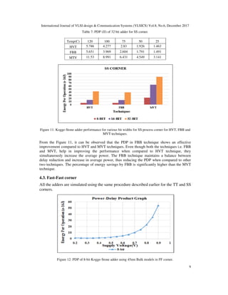
- 9. International Journal of VLSI design & Communication Systems (VLSICS) Vol.8, No.6, December 2017 9 Table 7: PDP (fJ) of 32 bit adder for SS corner. Temp(C) 120 100 75 50 25 HVT 5.786 4.277 2.83 1.926 1.463 FBB 5.651 3.969 2.604 1.791 1.491 MTV 11.53 8.991 6.431 4.549 3.141 Figure 11: Kogge-Stone adder performance for various bit widths for SS process corner for HVT, FBB and MVT techniques. From the Figure 11, it can be observed that the PDP in FBB technique shows an effective improvement compared to HVT and MVT techniques. Even though both the techniques i.e. FBB and MVT, help in improving the performance when compared to HVT technique, they simultaneously increase the average power. The FBB technique maintains a balance between delay reduction and increase in average power, thus reducing the PDP when compared to other two techniques. The percentage of energy savings by FBB is significantly higher than the MVT technique. 4.3. Fast-Fast corner All the adders are simulated using the same procedure described earlier for the TT and SS corners. Figure 12: PDP of 8-bit Kogge-Stone adder using 45nm Bulk models in FF corner.
- 10. International Journal of VLSI design & Communication Systems (VLSICS) Vol.8, No.6, December 2017 10 Figure 13: PDP of16-bit Kogge-Stone adder using 45nm Bulk models in FF corner. Figure 14: PDP of 32-bit Kogge-Stone adder using 45nm Bulk models in FF corner. Table 8: PDP (fJ) of 8 bit adder for FF corner. Temp(C) 120 100 75 50 25 HVT 13.07 9.67 6.53 4.457 3.211 FBB 12.82 9.62 6.38 4.37 3.12 MTV 136.42 119.15 94.69 67.93 54.77 Table 9: PDP (fJ) of 16 bit adder for FF corner. Temp(C) 120 100 75 50 25 HVT 36.57 26.98 18.15 12.31 8.8 FBB 35.02 26.2 17.31 11.77 8.39 MTV 157.6 143.13 108.7 83.2 65.1
- 11. International Journal of VLSI design & Communication Systems (VLSICS) Vol.8, No.6, December 2017 11 Table 10: PDP (fJ) of 32 bit adder for FF corner. Temp(C) 120 100 75 50 25 HVT 100.74 74.23 49.79 33.64 23.91 FBB 95.13 71.24 46.65 3.66 22.43 MTV 233.51 191.65 148.94 115.56 88.93 Figure 15: Kogge-Stone adder performance for various bit widths for FF process corner for HVT, FBB and MVT techniques. From the Figure 15, it can be observed that the PDP in FBB technique shows an effective improvement than HVT and MVT techniques. The FBB technique maintains a balance between delay reduction and increase in average power, thus reducing the PDP when compared to other two techniques. The percentage of energy savings by FBB is significantly higher than the MVT technique. 5. CONCLUSIONS The Kogge-Stone adder presented in this research work is efficient enough to operate in the sub- threshold region. Initially, the Kogge-Stone adder using HVT is efficiently employed for energy constrained operations using NCSU 45nm bulk CMOS process at SS, TT and FF corners operating in subthreshold region at a frequency of 50 KHz to obtain the minimum energy operating point. For better energy savings at the minimum operating point, performance improvement techniques such as forward body biasing and the use of multi threshold voltage transistors are explored. In forward body biasing technique, a body bias voltage is utilized which lowers the threshold voltage of the transistor cells which in turn improves the performance of the Kogge-Stone adder circuit. In the multi threshold voltage technique, in an adder circuit consisting of high threshold voltage cells, the low threshold voltage cells are placed in the critical path of the circuit to improve the performance of the Kogge-Stone adder circuit. Based on the comparative analysis performed, among all the three techniques discussed in this research work, the working of the Kogge-Stone adder in forward body bias technique proved to be both efficient and robust with a lower delay and power-delay product values compared to the other two techniques. In the subthreshold region of operation for a supply voltage of 0.3V, the adder had the least PDP. Even though the FBB technique exhibited the lower PDP values, HVT technique has marginally lower PDP. The PDP
- 12. International Journal of VLSI design & Communication Systems (VLSICS) Vol.8, No.6, December 2017 12 obtained using MVT was at least twice that of the PDP obtained using the FBB technique for all the adders. REFERENCES [1] Alice Wang , Benton Highsmith Calhoun , Chandrakasan. “Sub-threshold Design for Ultra-Low Power Systems”, Integrated Circuits and Systems, 2006th Edition. [2] Priya Gupta, Anu Gupta and Abhijit Asati, “Power-Aware Design of Logarithmic Prefix Adders in Sub-threshold Regime: A comparative Analysis”, International Conference on Information and Communication Technologies, 2015, pp. 1401-1408. [3] T. McPherson et al., “760 MHz G6 S/390 Microprocessor Exploiting Multiple V_t and Copper Interconnects,” Proceedings of the IEEE International Solid-State Circuits Conference, pp. 96-97, February 2000. [4] J.T. Kao and A. Chandrakasan, “Dual-Threshold Voltage Techniques for Low Power Digital Circuits,” IEEE Journal of Solid-State Circuits, Vol. 35, No. 7, pp. 1009-1018, July 2000. [5] A. Raychowdhury, B. C. Paul, S. Bhunia, and K. Roy, “Computing with sub-threshold leakage: Device/circuit/architecture co-design for ultralow power sub-threshold operation”, IEEE Trans. Very Large Scale Integr. (VLSI) Syst., vol. 13, no. 11, pp. 1213–1224, Nov. 2005. [6] J. P. Campbell, L. C. Yu, K. P. Cheung, J. Qin, J. S. Suehle, A. Oates, and K. Sheng, “Large random telegraph noise in sub-threshold operation of nano-scale n MOSFETs”, in Proc. IEEE Int. Conf. IC Design Technol., May 2009, pp. 17–20. [7] Priya Gupta, Anu Gupta and Abhijit Asati, “A Review on Ultra Low Power Design Technique: Subthreshold Logic”, International Journal of Computer Science and Technology, April-June 2013, pp. 64-71. [8] D.Bol, R.Ambroise, D.Flandre and J.D.Legat. “Interests and limitations of technology scaling for subthreshold logic,” IEEE Transactions on Very Large Scale Integration (VLSI) Systems, vol. 17, no. 10, pp. 1508–1519, 2009. [9] S. Narendra, D. Antoniadis, and V. De, “Impact of Using Adaptive Body Bias to Compensate Die-to- Die V_t Variation on Within-die V_t variation,” Proceedings of the IEEE International Symposium on Low Power Electronics and Design, pp. 229-232, August 1999. [10] A. Keshavarzi et al., “Technology Scaling Behavior of Optimum Reverse Body Bias for Standby Leakage Power Reduction in CMOS IC’s,” Proceedings of the IEEE International Symposium on Low Power Electronics and Design, pp. 252-254, July 1999. [11] C. Wann et al., “CMOS with Active Well Bias for Low Power and RF/Analog Applications,” Proceedings of the IEEE International Symposium on VLSI Technology, pp. 158-159, June 2000. [12] S. –F. Huang et al., “Scalability and Biasing Strategy for CMOS with Active Well Bias,” Proceedings of the IEEE International Symposium on VLSI Technology, pp. 107-108, June 2001. [13] Raghav, Himadri Singh, Sachin Maheswari, and B. Prasad Singh. "Performance Analysis of Subthreshold 32-Bit Kogge-Stone Adder for Worst-Case-Delay and Power in Sub-micron Technology." Communications in Computer and Information Science VLSI Design and Test (2013): 100-07. [14] Gupta, S. K., A. Raychowdhury and K. Roy. "Digital Computation in Subthreshold Region for Ultralow-Power Operation: A Device-Circuit-Architecture Codesign Perspective." Proceedings of the IEEE 98, no. 2 (2010): 160-190.
- 13. International Journal of VLSI design & Communication Systems (VLSICS) Vol.8, No.6, December 2017 13 AUTHORS Sruthi Nanduru received her M.S in Computer Engineering from the University of Texas at San Antonio in August 2016. She is currently working in Intel. Her research interests include, ultra low power computing, low power VLSI systems, computer architecture and performance evaluation. Santosh Koppa received his Ph. D. in Electrical Engineering from the University of Texas at San Antonio. He is currently working in Global Foundries US Inc. His research interests include, ultra low power analog and digital circuits, Internet of Things, low power VLSI systems. Eugene John received his Ph. D. in Electrical Engineering from the Pennsylvanian State University. He is currently a professor in the department of electrical and computer engineering. His research interests include, ultra-low power computing, low power VLSI systems, integrated circuit IP security and trust and computer architecture and performance evaluation