


INTERFACING 8051-MICROCONTROLLER with timer and display
- 1. UNIT V INTERFACING MICROCONTROLLER Dr. C.Helen Sulochana Professor/ECE
- 2. Programming 8051 Timers – Serial Port Programming – Interrupts Programming – LCD & Keyboard Interfacing – ADC, DAC & Sensor Interfacing , Stepper Motor and Waveform generation
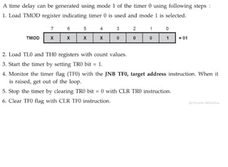
- 3. Programming 8051 TIMERS 8051 has two 16 bit timers, Timer 0, Timer 1. They operate as a counter or timer Since 8051 is 8-bit microcontroller each 16 bit registers are accessed as low-byte register(TL) and high byte Register(HL) 8051 Timer related registers 1. Timer Mode registers (TMOD) TMOD register configure the timers for the following operations Format of Timer mode register
- 5. 2. Timer control registers (TCON) Format of Timer control register
- 6. 8051 Timer modes and programming
- 7. 1. Mode 0- same for Timer 0 and 1 Mode 0 is 8bit counter with a divide–by-32 prescaler In this mode , Timer register is configured as a 13-bit register consists of 8 bits of TH1 and 5 bits of TL1 As the count rolls from all 1’s to all 0’s, it sets the timer interrupt flag IF1(in TCON) The counted input is enabled to the timer when TR1=1 and either GATE=0 or =1 TR1 is control bit in TCON, GATE is in TMOD
- 8. 2. Mode 1 Timer 0 -mode 1 programming
- 10. Timer 1 -mode 1 programming
- 11. 3. Mode 2 Timer 0 -mode 2 programming
- 12. Timer 1 -mode 2 programming
- 13. 4. Mode 3
- 16. Serial port programming -8051 Basics of Serial Communication Computers transfer data in two ways: Parallel: Often 8 or more lines (wire conductors) are used to transfer data to a device that is only a few feet away. Serial: To transfer to a device located many meters away, the serial method is used. The data is sent one bit at a time. •Serial data communication uses two methods Synchronous method transfers a block of data at a time Asynchronous method transfers a single byte at a time • There are special IC's made by many manufacturers for serial communications. UART (universal asynchronous Receiver transmitter) USART (universal synchronous-asynchronous Receiver- transmitter)8251 Extra
- 17. Asynchronous - Start & Stop Bit • Asynchronous serial data communication is widely used for character-oriented transmissions Each character is placed in between start and stop bits, this is called framing. Block-oriented data transfers use the synchronous method. • The start bit is always one bit, but the stop bit can be one or two bits • The start bit is always a 0 (low) and the stop bit(s) is 1 (high) Extra
- 18. Data Transfer Rate The rate of data transfer in serial data communication is stated in bps (bits per second). • Another widely used terminology for bps is baud rate. It is modem terminology and is defined as the number of signal changes per second In modems, there are occasions when a single change of signal transfers several bits of data • As far as the conductor wire is concerned, the baud rate and bps are the same. Extra
- 19. Registers related to Serial Communication •SBUF is an 8-bit register used solely for serial communication. •For a byte data to be transferred via the TxD line, it must be placed in the SBUF register. •The moment a byte is written into SBUF, it is framed with the start and stop bits and transferred serially via the TxD line. •SBUF holds the byte of data when it is received by 8051 RxD line. 1)SBUF - Serial Buffer Register • The SCON register in the 8051 microcontroller is an 8-bit register that controls serial communication. • 8051 provides four programmable modes for serial communication. A particular mode can be selected by setting the SM0 and SM1 bits in SCON. 2) SCON- Serial Control Register 8051 Serial Port is full duplex, transmit and receive simultaneously •It uses Register SBUF to hold the data •SCON Register is used to Control the data communication •Register –PCON to control the data rates •Pins RxD and TxD do the data transfer 8051 Serial Port programming
- 20. Bit pattern of SCON register SM0, SM1: Serial port mode bit 0, Serial port mode bit 1 SM2 :Serial port mode bit 2.. Enables multiprocessor communication. REN: (Receive enable) .Enables data reception. TB8: (Transmit bit 8 ) Transmits the 9th bit in modes 2,3. RB8: (Receive bit 8). Receives the 9th bit in modes 2, 3. TI: (Transmit interrupt flag) set when transmission is complete. RI: (Receive interrupt flag), set when byte is received
- 21. Bit pattern of PCON register 3. PCON (Power Control) Register •is an 8-bit register that controls power-saving modes and baud rate. SMOD (Serial Mode) – Bit 7: Doubles the baud rate for serial communication. Pins 6 to 4 –Not defined GF1 (General-purpose Flag 1) – Bit 3: User-defined flag for general purposes. GF0 (General-purpose Flag 0) – Bit 4: Another user-defined flag for general purposes. PD (Power Down) – Bit 1: Puts the microcontroller into power-down mode, halting the oscillator. IDL (Idle Mode) – Bit 0: Puts the CPU in idle mode, halting the CPU but allowing peripherals to run. Operating modes of Serial Communication 1. Mode 0 The Serial Port in Mode-0 has the following features: 1. Serial data enters and exits through RxD 2. TxD outputs the clock 3. 8 bits are transmitted/received 4. The baud rate is fixed at (1/12) of the oscillator frequency
- 22. 2. Mode 1 The Serial Port in Mode-1 has the following features: 1. Serial data enters through RxD 2. Serial data exits through TxD 3. On receive, the stop bit goes into RB8 in SCON 4. 10 bits are transmitted/ received as 1. Start bit (0) 2. 8 Data bits (LSB first) 3. Stop Bit (1) 5. Baud rate is determined by the Timer 1 over flow rate. The Serial Port in Mode-2 has the following features: 1. Serial data Received through RxD 2. Serial data Transmitted through TxD 3. 9th data bit (TB8) can be assign value 0 or 1. parity bit P in PSW is moved into TB8 4. On receive, the 9th data bit goes into RB8 in SCON, stop bit is ignored 5. 11 bits are transmitted/received 1.Start bit (0) 2. 8 Data bits (LSB first) 3. Programmable 9th data bit 3.Stop Bit (1) 6. Baud rate is programmable(1/32 or 1/64 the clock freuency) 3. Mode 2
- 23. The Serial Port in Mode-3 has the following features: 1. Serial data received through RxD 2. Serial data transmitted through TxD 3. 9th data bit (TB8) can be assign value 0 or 1 4. On receive, the 9th data bit goes into RB8 in SCON 5. 11 bits are transmitted/received 1.Start bit (0) 2. 8 Data bits (LSB first) 3. Programmable 9th data bit 3.Stop Bit (1) 6. Baud rate is determined by Timer 1 overflow rate.+ 3. Mode 3 Summary of modes
- 24. Programming Serial Data Transmission Following sequence of operation are performed to program Serial Data Transmission in 8051 1. TMOD register is loaded with the value 20H, indicating the use of timer 1 in mode 2 (8-bit auto-reload) to set baud rate. 2. The TH1 is loaded with one of the values to set baud rate for serial data transfer. 3. The SCON register is loaded with the value 50H, indicating serial mode 1, where an 8-bit data is framed with start and stop bits. 4. TR1 is set to 1 to start timer 1. 5. TI is cleared by CLR TI instruction. 6. The character byte to be sent is written into SBUF register. 7. The TI flag bit is monitored with the use of instruction JNB TI, XXXX to see if the character has been transferred completely. 8. To transfer the next byte, go to step 5 Programming Serial Data Reception 1. TMOD register is loaded with the value 20H, indicating the use of timer 1 in mode 2 (8- bit auto-reload) to set baud rate. 2. TH1 is loaded to set baud rate. 3. The SCON register is loaded with the value 50H, indicating serial mode 1, where an 8-bit data is framed with start and stop bits. 4. TR1 is set to 1 to start timer 1 5. RI is cleared by CLR RI instruction
- 25. 6. The RI flag bit is monitored with the use of instruction JNB RI, XXXX to see if an entire character has been received yet 7. When RI is raised, SBUF has the byte, its contents are moved into a safe place. 8. To receive the next character, go to step 5. Doubling Baud Rate There are two ways to increase the baud rate of data transfer 1. By using a higher frequency crystal 2. By changing a bit in the PCON register When 8051 is powered up, SMOD is zero We can set it to high by software and thereby double the baud rate. PCON register is an 8-bit register.
- 26. Interrupts Programming An interrupt is an external or internal event that interrupts the microcontroller to inform it that a device needs its service A single microcontroller can serve several devices by two ways: Interrupt Polling Interrupts Polling Whenever any device needs its service, the device notifies the microcontroller by sending it an interrupt signal. Upon receiving an interrupt signal, the microcontroller interrupts whatever it is doing and serves the device. The program which is associated with the interrupt is called the interrupt service routine (ISR) or interrupt handler. The microcontroller continuously monitors the status of a given device. When the conditions met, it performs the service. After that, it moves on to monitor the next device until every one is serviced. Can serve many devices (not all at the same time). not efficient, since it wastes much of the microcontroller’s time by polling devices that do not need service.
- 28. Types of Interrupts in 8051 Five sources of interrupts in 8051are: 1. Timer 0 overflow interrupt- TF0 2.Timer 1 overflow interrupt- TF1 1 and 2 are generated by TF0 and TF1, which are set by counter/reset register 3. External hardware interrupt- INT0 4.External hardware interrupt- INT1 3 and 4 can be activated depends on bits IT0 and IT1 in register TCON. The flags that generate theses interrupts are IE0 and IE1 in TCON 5. Serial communication interrupt- RI/TI 5 is generated by the logical OR of RI and TI The Timer and Serial interrupts are internally generated by the microcontroller, whereas the external interrupts are generated by additional interfacing devices or switches that are externally connected to the microcontroller The various registers associated with the use of interrupts are: TCON - Edge and Type bits for External Interrupts 0/1 SCON - RI and TI interrupt flags for RS232 IE - interrupt Enable IP - Specify priority of interrupts 8051 Interrupt related Registers
- 29. When 8051 is reset, all interrupts are disabled (masked), The interrupts are enabled by software Interrupt sources can be enabled or disabled by setting or clearing a bit in the special function register IE (interrupt enable) Interrupt control(Enabling and Disabling an Interrupt) interrupt enable Register
- 30. Interrupt priority and interrupt destination Each Interrupt source can be programmed to one of two priority level(low and high) by setting or clearing a bit in the register IP A low priority interrupt can be interrupted by high priority interrupt A high priority interrupt can not be interrupted by other low priority interrupt sources If two requests of different priority levels are received simultaneously, the request of highest priority level is served If two requests of same priority level are received simultaneously, an internal polling sequence determines which request is served Interrupt priority
- 31. Programming Interrupts 1. Programming Timer Interrupts Timer 0 and timer 1 interrupts are generated by TF0 and TF1, which are set by a rollover in the respective timer/counter, Timer flag(TF) is set(=1), when timer rolls over. TF is monitored with the instruction ‘JNB TF, target address’ and wait until TF is raised without doing anything in the polling method. In interrupt method, if the timer interrupt in the Interrupt enable register IE is enabled, TF is set whenever timer rolls over and 8051 is interrupted 2. Programming Hardware Interrupts ‘Pins P 3.2 and P 3.3 in port 3 are used as hardware interrupt and interrupt and can be either transition activated or level activated and are normally high. In level triggered mode, a low level signal applied to it trigger the interrupt In transition activated mode, a high to low level signal trigger the interrupt The flags that generate theses interrupts are IE0 and IE1 in TCON If ITx =0, external interrupt x is detected by a low at the pin If ITx =1, external interrupt x is detected by a high in one cycle and low in next cycle at the pin
- 32. 3. Programming Hardware Interrupts Serial communication interrupt is generated by the logical OR of RI and TI Transmit interrupt (TI) flag is set (=1), when stop bit is transmitted. This indicate that SBUF is ready to transmit the next byte. The receive interrupt flag(RI) is set (=1), when complete data is received IE register is enabled when RI or TI is set (=1), then 8051 is interrupted · The current Program Counter is saved on the stack, low-byte first. · Interrupts of the same and lower priority are blocked. · In the case of Timer and External interrupts, the corresponding interrupt flag is set. · Program execution transfers to the corresponding interrupt handler vector address. · The Interrupt Handler Routine executes. An interrupt ends when your program executes the RETI instruction. When the RETI instruction is executed the following actions are taken by the microcontroller: Two bytes are popped off the stack into the Program Counter to restore normal program execution. · Interrupt status is restored to its pre-interrupt status. What Happens When an Interrupt Occurs? What Happens When an Interrupt Ends?
- 33. LCD Interfacing LCD Module In 20 x 2 LCD display module, the display has 2 lines , each of 20 characters PIN diagram PIN detail
- 34. Interfacing LCD Module with 8051
- 35. Commands for LCD Module
- 37. KEYBOARD INTERFACING IN 8051 Here eight keys are individually connected to specific pins of port P1. Each port pin gives the status of key connected to that pin. When port pin is logic 1, key is open, otherwise key is closed. Simple Keyboard Interfacing program reads status of all keys by getting data through P1 and compares it with FFH to check whether all keys are open. If all keys are open, instruction compare sets the zero flag, and the program waits for key debounce. After waiting about 10 ms , program checks the P1 for key press. If key press is found, program waits for another 10 ms as a key debounce period. After key debounce period, program reads the keycode from P1.
- 38. Matrix Keyboard Interfacing In simple keyboard interface one input line is required to interface one key and this number will increase with number of keys. Therefore, this is not suitable when it is necessary to interface large number of keys. To reduce number of connections keys are arranged in the matrix form It requires two ports: an input port and an output port. Rows are connected to the input port referred to as returned lines, and columns are connected to the output port referred to as scan lines. , when all keys are open, row and column do not have any connection. When any key is pressed it shorts corresponding row and column. If the output line of this column is low, it makes corresponding row line low; otherwise the status o row line is high. The key is identified by data sent on the output port and input code received from the input port.
- 39. 4x4 Matrix keyboard connected to port 1 of 8051:
- 40. 1. Initialize P1.0, P1.1, P1.2, P1.3 as inputs i.e. write '1' to these pins. 2. Check if all the keys are released by writing '0' to P1.4-P1.7 and check if all return lines are in state '1'. If No then wait. If Yes then go to step 3. 3. Call debounce 4. Wait for key closure. Ground all scan lines by writing '0' and then check if at least one of return lines shows 'O' level. 5. Call debounce. (allow sufficient time for debounce) 6. Is key really pressed? (Ground all scan lines by writing '0' and then check if at least one of the return lines shows 'O' level.) No, step 4 Yes , step 7 7. Find key code and display the key pressed on 7-segment display. (By grounding one scan line at a time and checking return lines for any one line to go to '0' level. ) 8. Go to step 1. 4x4 matrix keyboard is connected to the port 1 of 8051 4 lines of port 1(p14-p17) are used scan lines Remaining 4 lines(P10-P13) are used as return lines Steps in algorithm for keyboard interface
- 41. The analog to digital converter chips 0808 and 0809 are 8-bit CMOS, successive approximation converters. conversion time. - the time taken to produce a valid output binary code for an applied input voltage. When we refer to a converter as high speed, it has a short conversion time. conversion delay is 100 µs at a clock frequency of 640 kHz do not need any external zero or full scale adjustments have a 3:8 analog multiplexer(at a time eight different analog inputs can be connected ) Out of these eight inputs only one can be selected for conversion by using address lines ADD A, ADD B and ADD C, Using these address inputs, ultichannel data acquisition system can be designed using a single ADC PIN diagram ADC -Interfacing
- 42. operation ADC has 8 input channels , 3 bit address line (A, B, C) is used to select the desired input channel The address must be latched for at least 50ns using Address latch enable (ALE) signal After 2.5 s , the Start Of Conversion(SOC) signal must be send high then low to start conversion process. End of conversion is indicated by End Of Conversion(EOC) signal Microprocessor can read the digital word by enabling the output enable signal. Timing diagram
- 44. Interfacing ADC with 8051 EOC=INTR 1.Select analog channel 2.Activate ALE 3.Activate SC 4.Monitor EOC 5.Activate OE
- 46. Digital to analog(DAC) -Interfacing D/A converter converts the digital signal into analog signal Several techniques are employed for digital to analog conversion. i. Weighted resistor network ii. R-2R ladder network iii. Current output D/A converter 1. Resolution: It is a change in analog output for one LSB change in digital input. the smallest increment of output that the DAC can produce for LSB change Resolution for n bit digital input is =(1/2n )*Vref. Vref = reference voltage eg. n=8 (i.e.8-bit DAC), Vref =5V’ then, resolution = 1/256*5V=39.06mV 2. Settling time: It is the time required for the DAC to settle from its initial output to steady state output(final value) Characteristics:
- 47. DAC require a reference analog voltage (Vref) or current (Iref) source. DAC0800 is available as a 16-pin IC in DIP DAC is an 8-bit, high speed, current output with settling time (conversion time) of 100 ns. It produces complementary current output, which can be converted to voltage by using simple resistor load. DAC require a positive and a negative supply voltage in the range of ± 5V to ±18V. Resolution of the DAC is 39.06mV Features: PIN diagram Interfacing DAC with 8051
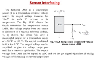
- 51. Sensor Interfacing with 8051 Note : Continue with ADC interfacing also
- 52. Stepper motor is a widely used device that translates electrical pulses into mechanical movement. Stepper motor is used in applications such as; disk drives, dot matrix printer, robotics etc It has a permanent magnet rotor called the shaft which is surrounded by a stator. stepper motor shafts move in fixed repeatable increments. Commonly used stepper motors have four stator windings. Such motors are called as four-phase or unipolar stepper motor. STEPPER MOTOR INTERFACING WITH 8051 Two phase motor is interfaces using 8051. The circuit has
- 54. Half step excitation (Digital locking system)
- 55. Step Angle − is the minimum degree of rotation with a single step. Steps per Revolution − This is the number of step angles required for a complete revolution. No of steps per revolution = 360° / step angle Steps per Second − This is number of steps covered in each second. Steps per second = (rpm x steps per revolution) / 60 rpm is the Revolution Per Minute. It measures the frequency of rotation. parameters of stepper motors 8051 interface with stepper motor
- 57. Waveform generation Note:- Write the content of DAC Interfacing then continue this Interfacing a DAC 0808/1408 with the 8051 microcontroller involves connecting the 8-bit digital output from the 8051's Port P1 to the DAC's input. The DAC converts this digital data into a corresponding analog signal, which can be used for applications like waveform generation or audio signal processing. Types of waveforms that we discuss here are as follows: Square wave Triangular wave Sine wave Square Wave A periodic waveform alternating between high and low is the square wave. To generate square wave first we have to output FF and then 00 on port1 of 8051. The port 1 is connected as an input to the DAC 0808. According to frequency requirement delay is provided between the two outputs. Role of Timers in Square Wave Generation 8051 Timer : The 8051 microcontroller has two timers: Timer 0 and Timer 1. These timers can be configured in different modes to generate specific time delays, which can be used to toggle an I/O pin.
- 58. Timer Modes: Mode 0: 13-bit timer mode (not commonly used for square wave generation) Mode 1: 16-bit timer mode (used for generating square waves) Mode 2: 8-bit auto-reload mode Mode 3: Split timer mode Mode 1 is generally used for generating square waves because it provides a wide range of delay values with high precision.
- 59. Triangular Wave To generate triangular wave we have to output data from 00 initially, and it should be cremented upto FF. When it reaches FF it should be decremented upto 00. Characteristics of a Triangular Wave Linear Rise and Fall: The amplitude of the signal increases linearly to a maximum value, then decreases linearly back to a minimum. Symmetry: A perfect triangular wave has equal rise and fall times, making it symmetric. Periodicity: The wave repeats itself over a constant period. A triangular wave is a type of waveform that rises and falls linearly, producing a shape resembling a triangle. In the context of the 8051 microcontroller, generating a triangular wave typically involves outputting a signal that incrementally increases in amplitude until it reaches a peak, and then decreases back to a minimum, repeating this process to form the wave.