Lecture Notes - Microprocessor - Unit 1 - Microprocessor Architecture and its operation
0 likes2,118 views
The document provides an overview of microprocessor architecture, focusing on the 8085 microprocessor, including its operation, internal components, and the functions it performs such as memory and I/O operations. It explains the roles of various buses (address, data, control) and the internal registers involved in executing instructions. Additionally, it discusses the differences between microprocessor-initiated operations and those triggered by peripheral devices.
1 of 33
Downloaded 73 times


Ad
Recommended
Introduction to microprocessor
Introduction to microprocessorKashyap Shah The document traces the history and development of microprocessors from 1971 to the present. It begins with the Intel 4004, the first commercial microprocessor released in 1971. Important subsequent microprocessors included the Intel 8080 in 1974 and 8085 in 1977. The Pentium brand was introduced in 1993 and included 64-bit x86 instruction sets. The Core 2 brand from 2006 featured single, dual, and quad-core processors. The document also provides basic explanations of how microprocessors work and their components like the ALU, registers, and control unit.
Types of instructions
Types of instructionsihsanjamil Types of instructions can be categorized into data transfer, arithmetic, and logical/program control instructions. Data transfer instructions like MOV copy data between registers and memory. Arithmetic instructions include INC/DEC to increment/decrement values, ADD/SUB for addition/subtraction, and MUL/DIV for multiplication/division. Logical instructions perform bitwise operations while program control instructions manage program flow.
Architecture of 8086 microprocessor
Architecture of 8086 microprocessorAnirban Saha Anik The document provides an overview of the 8086 microprocessor, introduced by Intel in 1978 as the first 16-bit microprocessor, highlighting its architecture which consists of a Bus Interface Unit (BIU) and Execution Unit (EU). It explains the main components and functions of each unit, including memory segmentation, general and special purpose registers, and the flag register. Additionally, it lists applications of the 8086 microprocessor in various devices such as gaming consoles, mobile phones, and household appliances.
Presentation on 8086 microprocessor
Presentation on 8086 microprocessorDiponkor Bala The document discusses the features and architecture of the Intel 8086 microprocessor, including its 16-bit architecture, 20-bit address bus, instruction queue, segmentation of memory into four 64KB segments, registers, flag register, arithmetic logic unit, and various addressing modes. It also provides a comparison of the 8086 to the 8085 microprocessor and describes some applications of the 8086.
Logical instruction of 8085
Logical instruction of 8085vishalgohel12195 The document provides an overview of the logical instruction set of the 8085 microprocessor, which includes 246 instructions classified into various categories such as data transfer, arithmetic, branching, control, and logical instructions. It details the operations performed by logical instructions, including AND, OR, XOR, rotate, compare, and complement, emphasizing how these operations interact with the accumulator and affect status flags. The document also includes examples of each instruction type and summarizes the role of compare and rotate instructions in manipulating data stored in registers and memory.
8086
8086Ravi Anand The 8086 microprocessor is a 16-bit CPU launched by Intel in 1978. It has a 16-bit data bus and 20-bit address bus, allowing it to access up to 1MB of memory. The 8086 architecture partitions the CPU logic into two functional units - the Bus Interface Unit which handles external transactions, and the Execution Unit which performs decoding and execution. This separation improves processing speed by allowing parallel instruction fetching and execution via pipelining. The 8086 uses memory segmentation to access more memory than its 16-bit registers allow, dividing the 1MB address space into 64KB segments addressed using segment and offset registers.
8085-microprocessor
8085-microprocessorATTO RATHORE The 8085 microprocessor is an 8-bit microprocessor introduced in 1976 as an updated version of the 8080. It has features like multiplexed address/data bus and interrupt pins. The 8085 consists of units like the accumulator, ALU, registers, program counter, stack pointer, flags, and instruction decoder. It uses flags to indicate arithmetic results and has interrupt controls. Registers are used for data, addressing, and instructions. The timing and control unit coordinates operations using a clock. Serial I/O is also supported.
Flag register 8086 assignment
Flag register 8086 assignmentZia3130 The flag register in the 8086 CPU contains 16 bits with each bit corresponding to a flip-flop that indicates the status of instructions. There are 9 active flags that serve different purposes - 6 are status flags reflecting results and 3 are control flags that enable/disable operations. The status flags indicate things like carry, parity, zero, sign, overflow while the control flags control tracing mode, interrupts, and direction of string operations.
Instruction codes and computer registers
Instruction codes and computer registersmahesh kumar prajapat This document describes a lecture on basic computer organization and design. It discusses:
- The basic components of a computer including a processor, memory, registers, and bus.
- The instruction format and addressing modes of instructions in the basic computer.
- The registers in the basic computer including the program counter, address register, and accumulator.
- How the common bus is used to transfer data between registers and memory.
- The basic computer's instruction set including memory and register reference instructions.
- How the control unit decodes instructions and generates control signals to implement operations.
Architecture OF 8085
Architecture OF 8085muneer.k This document provides an overview of the internal architecture and programming of the 8085 microprocessor. It describes the main components of the 8085 including the control unit, arithmetic logic unit, registers, flags, program counter, stack pointer, and buses. It also covers the 8085 pin descriptions and functional details. The document is intended as a tutorial on understanding the 8085 architecture and programming model.
Arduino and its hw architecture
Arduino and its hw architectureZeeshan Rafiq Arduino is an open-source microcontroller board and development environment that can sense the environment using inputs from sensors and affect its surroundings by controlling lights, motors, and other actuators. The document discusses the hardware architecture of Arduino, including the different types of Arduino boards, the components of an Arduino Uno board, and the architecture of the Atmega328 microcontroller chip used in Arduino boards. It describes the microcontroller's memory types including flash memory, SRAM, and EEPROM.
Configuration of bus topology in cisco packet tracer by Tanjilur Rahman
Configuration of bus topology in cisco packet tracer by Tanjilur RahmanTanjilurRahman6 This document provides instructions for configuring a bus topology network in Cisco Packet Tracer. It involves selecting PCs, laptops and switches, configuring the devices with valid IP addresses, and testing connectivity by sending a message and pinging between devices. The configuration was successful with 0% packet loss, demonstrating a functioning bus topology network.
Microprocessor
MicroprocessorAdarsh Barnwal The document is a presentation on an introduction to microprocessors. It defines a microprocessor as an electronic circuit that functions as the central processing unit (CPU) of a computer. It then discusses the main components and architecture of a microprocessor, including the timing and control unit, arithmetic logic unit, interface section, and register section. It provides examples of the 8085 microprocessor pin diagram and block diagram to illustrate these sections.
8085 addressing modes
8085 addressing modesVijay Kumar The document discusses the addressing modes used by the Intel 8085 microprocessor. It explains that an instruction specifies an operation along with the source and destination addresses. The Intel 8085 supports 5 addressing modes: direct, register, register indirect, immediate, and implicit. Each mode is defined by how the source or destination operand address is specified in the instruction.
Synchronous and-asynchronous-data-transfer
Synchronous and-asynchronous-data-transferAnuj Modi Synchronous data transfer involves sharing a common clock between a CPU and I/O interface so that data transfer is coordinated. Asynchronous transfer has independent clocks, so handshaking methods like strobe control and handshaking are used. Strobe control uses a single strobe pulse to indicate valid data. Handshaking adds a second control signal for acknowledgment between units. This ensures the source knows data was received and the destination knows data is available.
Instruction Set Architecture
Instruction Set ArchitectureDilum Bandara The document discusses instruction set architecture (ISA), which is part of computer architecture related to programming. It defines the native data types, instructions, registers, addressing modes, and other low-level aspects of a computer's operation. Well-known ISAs include x86, ARM, MIPS, and RISC. A good ISA lasts through many implementations, supports a variety of uses, and provides convenient functions while permitting efficient implementation. Assembly language is used to program at the level of an ISA's registers, instructions, and execution order.
Microprocessor application (Introduction)
Microprocessor application (Introduction)Ismail Mukiibi The document discusses microprocessors, explaining their structure, functionality, and the types of instructions they execute. Key elements include the program counter, memory addressing, and various instruction types such as arithmetic, logical, branching, and data transfer. It also covers the 8086 microprocessor architecture, memory management, and interrupt handling in detail.
Microprocessor and Microcontroller Lab Manual!
Microprocessor and Microcontroller Lab Manual!PRABHAHARAN429 The document describes experiments to be performed on an 8-bit microprocessor and microcontroller. It includes aims, block diagrams, flowcharts and assembly language programs for arithmetic operations, sorting an array, and interfacing experiments. Experiments cover topics like addition, subtraction, multiplication, division, ascending/descending order, maximum/minimum values, and interfacing components like ADCs, DACs, stepper motors. Similar experiments are outlined for an 8-bit microcontroller.
Instruction cycle of computer
Instruction cycle of computerA. S. M. Shafi A processor has an instruction set that defines the basic operations it can perform. An instruction set includes instructions, registers, addressing modes, and memory architecture. Two processors are only compatible if they have the same instruction set. The primary responsibility of a CPU is to execute instructions that make up a program. It does this through an instruction cycle that involves fetching an instruction from memory, decoding it, executing the operation, and storing the results back in memory. Instructions can perform memory transfers, arithmetic, logic, and control operations. A CPU's performance is measured by the number of instructions it can execute per second.
CH4.ppt
CH4.pptSharanKumarHuli1 This chapter discusses data movement instructions in x86 assembly language. It covers common instructions like MOV, PUSH, POP and string instructions. It explains how instructions are represented in machine code, including opcode, operands, addressing modes, registers, and data sizes. Special emphasis is placed on interpreting unknown machine code and correctly representing symbolic instructions in binary. The goal is for readers to understand how to select the proper instruction to accomplish data transfers and translate between assembly mnemonics and machine language.
8051 Architecture
8051 ArchitectureShinuMMAEI The document provides a comprehensive overview of the 8051 microcontroller architecture, contrasting it with microprocessors and discussing their respective characteristics, such as internal memory, power consumption, and processing speed. It details the pin configuration, internal registers, and operation modes of the 8051 microcontroller, emphasizing its embedded system applications. Key differences between microcontrollers and embedded processors are also highlighted, focusing on integration, cost, and functionality.
8155 Basic Concepts
8155 Basic ConceptsSrinath Kalikivayi The document discusses the 8155 programmable interface device. The 8155 can be used to interface I/O devices to a microprocessor like the 8085. It contains 256 bytes of RAM, three I/O ports (Ports A, B, and C), and a 14-bit timer. The 8155 is programmed by the 8085 which sends data and instruction words to configure the I/O ports and timer registers. The timer on the 8155 has two registers and can operate in four modes to generate different output waveforms.
Introduction to 8085 microprocessor
Introduction to 8085 microprocessorkunj desai The document provides an introduction to the Intel 8085 microprocessor. It describes the 8085 as an 8-bit microprocessor introduced by Intel in 1977 as an extension of the 8080. The 8085 requires only a single +5V power supply. It has 8-bit data bus, 16-bit address bus, and can operate at speeds up to 5MHz. The document outlines the basic components, architecture, and features of the 8085, including its register section, ALU, interrupt control, instruction decoding, and I/O capabilities.
Computer instruction
Computer instructionSanjeev Patel 1. The document discusses the topics of computer instructions, timing and control, and the instruction cycle for a basic computer.
2. It describes the three instruction code formats used - memory reference, register reference, and input/output. Memory reference instructions use bits to specify an address and addressing mode. Register reference instructions specify an operation on the accumulator register.
3. The instruction cycle consists of four phases - fetch an instruction, decode the instruction, read the effective address if needed, and execute the instruction.
Memory interfacing of microprocessor 8085
Memory interfacing of microprocessor 8085Nilesh Bhaskarrao Bahadure The document provides an in-depth overview of memory interfacing with the microprocessor 8085, covering semiconductor memory fundamentals, types, and structures. It discusses memory decoding techniques, input/output interfacing, and examples of interfacing different memory configurations and I/O devices. Furthermore, it explains the contrasts between memory-mapped I/O and I/O mapped I/O, detailing various data transfer methods within the context of microprocessor systems.
8155 GPPI
8155 GPPIdeval patel The document discusses the 8155 Programmable Peripheral Interface chip. It can be used as an interface between a microprocessor and I/O devices. The 8155 contains RAM, I/O ports, and a timer. It has ports A, B, and C that can be configured as input or output. The timer can operate in different modes. Programming the 8155 involves writing control words to its control register to configure the ports and timer. An example application shows how an 8155 can be used to interface an ADC and read temperature values using handshaking between the ADC and 8155 ports.
REGISTER TRANSFER AND MICRO OPERATIONS
REGISTER TRANSFER AND MICRO OPERATIONSAnonymous Red This document discusses register transfer language and microoperations. It begins by defining register transfer language as the symbolic notation used to describe transfers between registers using hardware logic circuits. It describes two common ways to transfer information: directly between registers using a replacement operator (R2 ! R1), and conditionally using an if-then statement (if P=1 then R2 ! R1). The document then discusses various microoperations including arithmetic operations like addition and subtraction, as well as incrementing and decrementing registers. It also covers transferring data to and from memory and constructing common bus systems using multiplexers or three-state buffers to transfer data between multiple registers.
architect.ppt
architect.pptSELVAPRIYAA2 The document discusses the architecture and operation of the Intel 8085 microprocessor. It describes the 8085's internal functional blocks like the accumulator, program counter, stack pointer, and flags register. It explains the different types of operations the 8085 can perform, including memory/I/O read/write operations initiated by the microprocessor. It provides details on the 8085's external pinouts, including the address bus, data bus, control signals, and clock inputs. It discusses bus timing and the sequence of signals involved in fetching an instruction from memory. Finally, it introduces concepts like T-states, machine cycles, and instruction cycles.
Lecture Notes Microprocessor and Controller Unit2
Lecture Notes Microprocessor and Controller Unit2Murugan146644 Lecture Notes - Microprocessor - Unit 2 - 8085 Pinout signal, Functional Block Diagram and Instruction Set
Description:
Welcome to the comprehensive guide on Microprocessor and micro controller tailored for First year (Second Semester) B.Sc. Computer Science students affiliated with Alagappa University. This document covers fundamental concepts of microprocessor and micro controller. PDF content is prepared from the text book R. S. Gaonkar- "Microprocessor Architecture- Programming and Applications with 8085"- 5th Edition
Key Topics Covered:
Main Topic : Pinout signal, Functional Block Diagram and Instruction Set
Sub-Topic :
The 8085 MPU - The 8085 Pinout Signal - (Address bus, Data bus, Control and Status Signal, Power supply and frequency signal, Externally Initiated Signals, Serial I/O ports), Functional Block Diagram - (The ALU, Timing and control unit, Instruction Register and Decoder - Instruction Set - Instruction Classification - (Data Transfer operation- Arithmetic operations - logical operations - branching operations - machine control operations)
Previous Link:
Unit I : https://www.slideshare.net/slideshow/lecture-notes-microprocessor-unit-1-microprocessor-architecture-and-its-operation/274981732
Target Audience:
First year (Second Semester) B.Sc. Computer Science students at Alagappa University seeking a solid foundation in microprocessor and micro controller for academic and practical applications.
About the Author:
Dr. S. Murugan is Associate Professor at Alagappa Government Arts College, Karaikudi. With more than 20 years of teaching experience in the field of Computer Science, Dr. S. Murugan has a passion for simplifying complex concepts in microprocessor and micro controller.
Disclaimer:
This document is intended for educational purposes only. The content presented here reflects the author’s understanding in the field of Microprocessor and micro controller.
Microprocessor and Microcontroller.pptx
Microprocessor and Microcontroller.pptxpvg123456 The document provides an overview of microprocessors and microcontrollers. It discusses the basic concepts of microprocessors including the definition, components like the ALU, registers, control unit, memory and system bus. It describes how a microprocessor works and introduces machine language and 8085 assembly language. The later lectures discuss the internal architecture, registers, pin configuration and instruction set of the 8085 microprocessor. It also covers addressing modes, classification of instructions and use of the stack in 8085.
More Related Content
What's hot (19)
Instruction codes and computer registers
Instruction codes and computer registersmahesh kumar prajapat This document describes a lecture on basic computer organization and design. It discusses:
- The basic components of a computer including a processor, memory, registers, and bus.
- The instruction format and addressing modes of instructions in the basic computer.
- The registers in the basic computer including the program counter, address register, and accumulator.
- How the common bus is used to transfer data between registers and memory.
- The basic computer's instruction set including memory and register reference instructions.
- How the control unit decodes instructions and generates control signals to implement operations.
Architecture OF 8085
Architecture OF 8085muneer.k This document provides an overview of the internal architecture and programming of the 8085 microprocessor. It describes the main components of the 8085 including the control unit, arithmetic logic unit, registers, flags, program counter, stack pointer, and buses. It also covers the 8085 pin descriptions and functional details. The document is intended as a tutorial on understanding the 8085 architecture and programming model.
Arduino and its hw architecture
Arduino and its hw architectureZeeshan Rafiq Arduino is an open-source microcontroller board and development environment that can sense the environment using inputs from sensors and affect its surroundings by controlling lights, motors, and other actuators. The document discusses the hardware architecture of Arduino, including the different types of Arduino boards, the components of an Arduino Uno board, and the architecture of the Atmega328 microcontroller chip used in Arduino boards. It describes the microcontroller's memory types including flash memory, SRAM, and EEPROM.
Configuration of bus topology in cisco packet tracer by Tanjilur Rahman
Configuration of bus topology in cisco packet tracer by Tanjilur RahmanTanjilurRahman6 This document provides instructions for configuring a bus topology network in Cisco Packet Tracer. It involves selecting PCs, laptops and switches, configuring the devices with valid IP addresses, and testing connectivity by sending a message and pinging between devices. The configuration was successful with 0% packet loss, demonstrating a functioning bus topology network.
Microprocessor
MicroprocessorAdarsh Barnwal The document is a presentation on an introduction to microprocessors. It defines a microprocessor as an electronic circuit that functions as the central processing unit (CPU) of a computer. It then discusses the main components and architecture of a microprocessor, including the timing and control unit, arithmetic logic unit, interface section, and register section. It provides examples of the 8085 microprocessor pin diagram and block diagram to illustrate these sections.
8085 addressing modes
8085 addressing modesVijay Kumar The document discusses the addressing modes used by the Intel 8085 microprocessor. It explains that an instruction specifies an operation along with the source and destination addresses. The Intel 8085 supports 5 addressing modes: direct, register, register indirect, immediate, and implicit. Each mode is defined by how the source or destination operand address is specified in the instruction.
Synchronous and-asynchronous-data-transfer
Synchronous and-asynchronous-data-transferAnuj Modi Synchronous data transfer involves sharing a common clock between a CPU and I/O interface so that data transfer is coordinated. Asynchronous transfer has independent clocks, so handshaking methods like strobe control and handshaking are used. Strobe control uses a single strobe pulse to indicate valid data. Handshaking adds a second control signal for acknowledgment between units. This ensures the source knows data was received and the destination knows data is available.
Instruction Set Architecture
Instruction Set ArchitectureDilum Bandara The document discusses instruction set architecture (ISA), which is part of computer architecture related to programming. It defines the native data types, instructions, registers, addressing modes, and other low-level aspects of a computer's operation. Well-known ISAs include x86, ARM, MIPS, and RISC. A good ISA lasts through many implementations, supports a variety of uses, and provides convenient functions while permitting efficient implementation. Assembly language is used to program at the level of an ISA's registers, instructions, and execution order.
Microprocessor application (Introduction)
Microprocessor application (Introduction)Ismail Mukiibi The document discusses microprocessors, explaining their structure, functionality, and the types of instructions they execute. Key elements include the program counter, memory addressing, and various instruction types such as arithmetic, logical, branching, and data transfer. It also covers the 8086 microprocessor architecture, memory management, and interrupt handling in detail.
Microprocessor and Microcontroller Lab Manual!
Microprocessor and Microcontroller Lab Manual!PRABHAHARAN429 The document describes experiments to be performed on an 8-bit microprocessor and microcontroller. It includes aims, block diagrams, flowcharts and assembly language programs for arithmetic operations, sorting an array, and interfacing experiments. Experiments cover topics like addition, subtraction, multiplication, division, ascending/descending order, maximum/minimum values, and interfacing components like ADCs, DACs, stepper motors. Similar experiments are outlined for an 8-bit microcontroller.
Instruction cycle of computer
Instruction cycle of computerA. S. M. Shafi A processor has an instruction set that defines the basic operations it can perform. An instruction set includes instructions, registers, addressing modes, and memory architecture. Two processors are only compatible if they have the same instruction set. The primary responsibility of a CPU is to execute instructions that make up a program. It does this through an instruction cycle that involves fetching an instruction from memory, decoding it, executing the operation, and storing the results back in memory. Instructions can perform memory transfers, arithmetic, logic, and control operations. A CPU's performance is measured by the number of instructions it can execute per second.
CH4.ppt
CH4.pptSharanKumarHuli1 This chapter discusses data movement instructions in x86 assembly language. It covers common instructions like MOV, PUSH, POP and string instructions. It explains how instructions are represented in machine code, including opcode, operands, addressing modes, registers, and data sizes. Special emphasis is placed on interpreting unknown machine code and correctly representing symbolic instructions in binary. The goal is for readers to understand how to select the proper instruction to accomplish data transfers and translate between assembly mnemonics and machine language.
8051 Architecture
8051 ArchitectureShinuMMAEI The document provides a comprehensive overview of the 8051 microcontroller architecture, contrasting it with microprocessors and discussing their respective characteristics, such as internal memory, power consumption, and processing speed. It details the pin configuration, internal registers, and operation modes of the 8051 microcontroller, emphasizing its embedded system applications. Key differences between microcontrollers and embedded processors are also highlighted, focusing on integration, cost, and functionality.
8155 Basic Concepts
8155 Basic ConceptsSrinath Kalikivayi The document discusses the 8155 programmable interface device. The 8155 can be used to interface I/O devices to a microprocessor like the 8085. It contains 256 bytes of RAM, three I/O ports (Ports A, B, and C), and a 14-bit timer. The 8155 is programmed by the 8085 which sends data and instruction words to configure the I/O ports and timer registers. The timer on the 8155 has two registers and can operate in four modes to generate different output waveforms.
Introduction to 8085 microprocessor
Introduction to 8085 microprocessorkunj desai The document provides an introduction to the Intel 8085 microprocessor. It describes the 8085 as an 8-bit microprocessor introduced by Intel in 1977 as an extension of the 8080. The 8085 requires only a single +5V power supply. It has 8-bit data bus, 16-bit address bus, and can operate at speeds up to 5MHz. The document outlines the basic components, architecture, and features of the 8085, including its register section, ALU, interrupt control, instruction decoding, and I/O capabilities.
Computer instruction
Computer instructionSanjeev Patel 1. The document discusses the topics of computer instructions, timing and control, and the instruction cycle for a basic computer.
2. It describes the three instruction code formats used - memory reference, register reference, and input/output. Memory reference instructions use bits to specify an address and addressing mode. Register reference instructions specify an operation on the accumulator register.
3. The instruction cycle consists of four phases - fetch an instruction, decode the instruction, read the effective address if needed, and execute the instruction.
Memory interfacing of microprocessor 8085
Memory interfacing of microprocessor 8085Nilesh Bhaskarrao Bahadure The document provides an in-depth overview of memory interfacing with the microprocessor 8085, covering semiconductor memory fundamentals, types, and structures. It discusses memory decoding techniques, input/output interfacing, and examples of interfacing different memory configurations and I/O devices. Furthermore, it explains the contrasts between memory-mapped I/O and I/O mapped I/O, detailing various data transfer methods within the context of microprocessor systems.
8155 GPPI
8155 GPPIdeval patel The document discusses the 8155 Programmable Peripheral Interface chip. It can be used as an interface between a microprocessor and I/O devices. The 8155 contains RAM, I/O ports, and a timer. It has ports A, B, and C that can be configured as input or output. The timer can operate in different modes. Programming the 8155 involves writing control words to its control register to configure the ports and timer. An example application shows how an 8155 can be used to interface an ADC and read temperature values using handshaking between the ADC and 8155 ports.
REGISTER TRANSFER AND MICRO OPERATIONS
REGISTER TRANSFER AND MICRO OPERATIONSAnonymous Red This document discusses register transfer language and microoperations. It begins by defining register transfer language as the symbolic notation used to describe transfers between registers using hardware logic circuits. It describes two common ways to transfer information: directly between registers using a replacement operator (R2 ! R1), and conditionally using an if-then statement (if P=1 then R2 ! R1). The document then discusses various microoperations including arithmetic operations like addition and subtraction, as well as incrementing and decrementing registers. It also covers transferring data to and from memory and constructing common bus systems using multiplexers or three-state buffers to transfer data between multiple registers.
Similar to Lecture Notes - Microprocessor - Unit 1 - Microprocessor Architecture and its operation (20)
architect.ppt
architect.pptSELVAPRIYAA2 The document discusses the architecture and operation of the Intel 8085 microprocessor. It describes the 8085's internal functional blocks like the accumulator, program counter, stack pointer, and flags register. It explains the different types of operations the 8085 can perform, including memory/I/O read/write operations initiated by the microprocessor. It provides details on the 8085's external pinouts, including the address bus, data bus, control signals, and clock inputs. It discusses bus timing and the sequence of signals involved in fetching an instruction from memory. Finally, it introduces concepts like T-states, machine cycles, and instruction cycles.
Lecture Notes Microprocessor and Controller Unit2
Lecture Notes Microprocessor and Controller Unit2Murugan146644 Lecture Notes - Microprocessor - Unit 2 - 8085 Pinout signal, Functional Block Diagram and Instruction Set
Description:
Welcome to the comprehensive guide on Microprocessor and micro controller tailored for First year (Second Semester) B.Sc. Computer Science students affiliated with Alagappa University. This document covers fundamental concepts of microprocessor and micro controller. PDF content is prepared from the text book R. S. Gaonkar- "Microprocessor Architecture- Programming and Applications with 8085"- 5th Edition
Key Topics Covered:
Main Topic : Pinout signal, Functional Block Diagram and Instruction Set
Sub-Topic :
The 8085 MPU - The 8085 Pinout Signal - (Address bus, Data bus, Control and Status Signal, Power supply and frequency signal, Externally Initiated Signals, Serial I/O ports), Functional Block Diagram - (The ALU, Timing and control unit, Instruction Register and Decoder - Instruction Set - Instruction Classification - (Data Transfer operation- Arithmetic operations - logical operations - branching operations - machine control operations)
Previous Link:
Unit I : https://www.slideshare.net/slideshow/lecture-notes-microprocessor-unit-1-microprocessor-architecture-and-its-operation/274981732
Target Audience:
First year (Second Semester) B.Sc. Computer Science students at Alagappa University seeking a solid foundation in microprocessor and micro controller for academic and practical applications.
About the Author:
Dr. S. Murugan is Associate Professor at Alagappa Government Arts College, Karaikudi. With more than 20 years of teaching experience in the field of Computer Science, Dr. S. Murugan has a passion for simplifying complex concepts in microprocessor and micro controller.
Disclaimer:
This document is intended for educational purposes only. The content presented here reflects the author’s understanding in the field of Microprocessor and micro controller.
Microprocessor and Microcontroller.pptx
Microprocessor and Microcontroller.pptxpvg123456 The document provides an overview of microprocessors and microcontrollers. It discusses the basic concepts of microprocessors including the definition, components like the ALU, registers, control unit, memory and system bus. It describes how a microprocessor works and introduces machine language and 8085 assembly language. The later lectures discuss the internal architecture, registers, pin configuration and instruction set of the 8085 microprocessor. It also covers addressing modes, classification of instructions and use of the stack in 8085.
architecture memory interfacing
architecture memory interfacingShamsul Huda The document provides an overview of the 8085 microprocessor architecture, detailing its components, operation, and interfacing methods. It explains the roles of the address bus, data bus, and control bus, as well as the internal architecture including registers and arithmetic logic unit. Additionally, it discusses memory organization, the concept of memory-mapped versus peripheral-mapped I/O, and outlines the processes for memory and I/O operations.
Unit 2.ppt
Unit 2.pptsharonmarishkawilfre The document discusses the architecture of the 8085 microprocessor. It describes the three busses - address bus, data bus, and control bus. It explains how the address bus is used to access memory locations, and how the data bus is used to transfer data. It also discusses the different types of operations the 8085 can perform, such as memory read/write, I/O read/write, internal operations, and externally initiated operations like reset and interrupts. The document provides details on the internal architecture of 8085 including registers, accumulator, program counter, and stack pointer. It concludes by describing the different addressing modes and instructions sets of 8085.
8085 MICROPROCESSOR ARCHITECTURE AND ITS OPERATIONS
8085 MICROPROCESSOR ARCHITECTURE AND ITS OPERATIONSRamaPrabha24 This document discusses the architecture and operations of microprocessors. It focuses on the Intel 8085 microprocessor. The 8085 architecture consists of a register array, ALU and logic group, instruction decoder and encoder, interrupt control group, and serial I/O control group. The register array contains general purpose registers, temporary registers, special purpose registers like the accumulator, flags register, and instruction register, and 16-bit registers like the program counter and stack pointer. The ALU performs arithmetic and logical operations. The instruction decoder decodes instructions and the timing and control circuitry manages the sequencing of operations. Microprocessor operations include memory reads/writes, I/O reads/writes using address, data and control buses, internal data operations
8085
8085Mohammed Khan This document provides an overview of the internal architecture and programming of the 8085 microprocessor. It describes the main components of the 8085 including the control unit, arithmetic logic unit, registers, flags, program counter, stack pointer, and buses. It also covers the 8085 pin descriptions and functional details. The document is an introduction to understanding the 8085 architecture and programming model.
8085
8085Donika Markande This document provides an overview of the internal architecture and programming of the 8085 microprocessor. It describes the main components of the 8085 including the control unit, arithmetic logic unit, registers, flags, program counter, stack pointer, and buses. It also covers the 8085 pin descriptions and functional details. The document is intended as a tutorial on understanding the 8085 architecture and programming model.
8085 microprocessor
8085 microprocessorgohanraw This document provides an overview of the internal architecture and programming of the 8085 microprocessor. It describes the main components of the 8085 including the control unit, arithmetic logic unit, registers, flags, program counter, stack pointer, and buses. It also covers the 8085 pin descriptions and functional details. The document is intended as a tutorial on understanding the 8085 architecture and programming model.
Unit 2 - Microprocessor & Microcontroller.pptx
Unit 2 - Microprocessor & Microcontroller.pptxCharunnath S V The document discusses the architecture of the 8085 microprocessor. It describes the main parts as the ALU, register set, timing and control unit, interrupt control, serial I/O control, and the instruction decoder and machine cycle encoder. The ALU performs arithmetic and logic operations. The register set includes general purpose, temporary, flag and special purpose registers like the program counter and stack pointer. The timing and control unit provides timing and control signals. Interrupt control handles software and hardware interrupts. Serial I/O control manages serial communication. The instruction decoder decodes instructions and the machine cycle encoder indicates the executing machine cycle.
8085 (1)
8085 (1)Mani Kandan K The document provides an overview of the Intel 8085 microprocessor architecture. It discusses the 8085's pins, buses, control signals, arithmetic logic unit, flags register, and memory interfacing. The 8085 uses an 8-bit address bus and 8-bit bi-directional data bus. It has pins for power, clock signals, interrupts and I/O. The document explains the 8085's opcode fetch, memory read/write and I/O read/write machine cycles and timing. It also covers addressing memory chips, interrupt handling and putting the concepts together in a system diagram.
MPMC UNIT-1. Microprocessor 8085 pdf Microprocessor and Microcontroller
MPMC UNIT-1. Microprocessor 8085 pdf Microprocessor and MicrocontrollerRAHUL RANJAN The document outlines the history, architecture, and functionality of microprocessors, starting from the invention of transistors and integrated circuits leading to Intel's development of the first microprocessor, the Intel 4004. It describes key components of the 8085 microprocessor, including its ALU, registers, address and data busses, and the various types of microprocessors based on data bus size and application. Additionally, it provides an overview of the operational and functional characteristics of the 8085 microprocessor along with its pin descriptions and control signals.
12 mt06ped001
12 mt06ped001 vijaydeepakg The document discusses the architecture of the 8085 microprocessor. It describes that the 8085 is an 8-bit microprocessor introduced by Intel in the mid-1970s. It has 40 pins and can address up to 64KB of memory. The 8085 uses three buses - address bus, data bus, and control/status bus - to perform memory read, memory write, I/O read, and I/O write operations. It has registers like accumulator, flags, program counter, stack pointer and temporary registers. The arithmetic logic unit performs arithmetic and logic operations. It also describes the address buffer, interrupt control, and serial I/O capabilities of the 8085 microprocessor.
UNIT 1 Microprocessors.pptx
UNIT 1 Microprocessors.pptxGowrishankar C The document provides information about the 8085 microprocessor, including its architecture, features, instruction formats, and addressing modes. The 8085 is an 8-bit microprocessor with an accumulator, registers, arithmetic logic unit (ALU), flags, and I/O controls. It has three types of instructions that are 1, 2, or 3 bytes long. The addressing modes allow instructions to specify operands and include immediate, direct, register, register indirect, and implicit modes.
PPT-1.pptx
PPT-1.pptxAnsal Valappil The document discusses the 8085 microprocessor architecture and pin configuration. It contains the following key points:
1. The 8085 has 40 pins that are divided into groups for the address bus, data bus, control signals, power/clock, interrupts, and serial I/O.
2. The address bus is multiplexed with the lower 8 bits of the data bus. Control signals like ALE are needed to demultiplex these.
3. The internal architecture of the 8085 includes an ALU, timing/control unit, instruction register, register array, and components for interrupts and serial I/O.
4. A single board computer system can be built around the 8085 to demonstrate its
PPT-1.pptx
PPT-1.pptxAnsal Valappil The document discusses the 8085 microprocessor architecture and pin configuration. It contains the following key points:
1. The 8085 has 40 pins that are divided into groups for the address bus, data bus, control signals, power/clock, interrupts, and serial I/O.
2. The address bus is multiplexed with the lower data lines, requiring demultiplexing. Control signals like RD, WR are used to indicate read/write operations.
3. The internal architecture of the 8085 includes an ALU, registers, interrupt and serial I/O control, and timing/control units.
4. Examples are given of memory access cycles and communication between the 8085 and external memory
Mechatronics UNIT 2.pptx
Mechatronics UNIT 2.pptxssuser823c58 The 8085 microprocessor has an address bus with 16 lines to identify memory locations and peripheral devices. It has an 8-line bi-directional data bus to transfer data. The control bus carries synchronization and timing signals. The 8085 has six general-purpose registers, an accumulator, flags register, program counter, stack pointer, and temporary register. The arithmetic logic unit performs operations using data from the accumulator and registers.
Introduction of CPU part 2
Introduction of CPU part 2Tharindu Darshana The document provides an overview of microprocessor architecture and the Intel 8085 microprocessor. It discusses that a microprocessor can be programmed to perform functions on data by writing instructions to memory. The microprocessor reads one instruction at a time to perform the specified data manipulation, storing results back in memory or displaying them. It then describes the architecture of the Intel 8085, including its 16-bit address bus, 8-bit bi-directional data bus, and control bus composed of single-bit signals. The document also outlines different types of microprocessor operations like memory reads/writes and I/O reads/writes, as well as internal operations involving registers, accumulators, and flags.
Computer system architecture (microprocessor 8085) unit 4
Computer system architecture (microprocessor 8085) unit 4Anjaan Gajendra The document provides an in-depth overview of the Intel 8085 microprocessor architecture, detailing its components such as registers, the arithmetic and logic unit, and the timing control unit. It discusses the system bus configuration and the various pin descriptions of the 8085, along with the types of operations the microprocessor can perform. Additionally, it highlights the evolution of microprocessors leading up to the introduction of the 8085 and its widespread use in computing.
Ad
More from Murugan146644 (20)
Computer Network Unit IV - Lecture Notes - Network Layer
Computer Network Unit IV - Lecture Notes - Network LayerMurugan146644 Title:
Lecture Notes - Unit IV - The Network Layer
Description:
Welcome to the comprehensive guide on Computer Network concepts, tailored for final year B.Sc. Computer Science students affiliated with Alagappa University. This document covers fundamental principles and advanced topics in Computer Network. PDF content is prepared from the text book Computer Network by Andrew S. Tenanbaum
Key Topics Covered:
Main Topic : The Network Layer
Sub-Topic : Network Layer Design Issues (Store and forward packet switching , service provided to the transport layer, implementation of connection less service, implementation of connection oriented service, Comparision of virtual circuit and datagram subnet), Routing algorithms (Shortest path routing, Flooding , Distance Vector routing algorithm, Link state routing algorithm , hierarchical routing algorithm, broadcast routing, multicast routing algorithm)
Other Link :
1.Introduction to computer network - https://www.slideshare.net/slideshow/lecture-notes-introduction-to-computer-network/274183454
2. Physical Layer - https://www.slideshare.net/slideshow/lecture-notes-unit-ii-the-physical-layer/274747125
3. Data Link Layer Part 1 : https://www.slideshare.net/slideshow/lecture-notes-unit-iii-the-datalink-layer/275288798
Target Audience:
Final year B.Sc. Computer Science students at Alagappa University seeking a solid foundation in Computer Network principles for academic.
About the Author:
Dr. S. Murugan is Associate Professor at Alagappa Government Arts College, Karaikudi. With 23 years of teaching experience in the field of Computer Science, Dr. S. Murugan has a passion for simplifying complex concepts in Computer Network
Disclaimer:
This document is intended for educational purposes only. The content presented here reflects the author’s understanding in the field of Computer Network
Assembly Language Program for 16_bit_Addition
Assembly Language Program for 16_bit_AdditionMurugan146644 User Manual - Microprocessor and Micro Controller Lab
Assembly Language Program for 16 bit addition
Previous Link:
Lab:
ALP Development and Execution Procedure : https://www.slideshare.net/slideshow/assembly-language-program-development-and-execution-procedure/275956545#2
Exercises:
1. 8 Bit Addition : https://www.slideshare.net/slideshow/assembly-language-program-for-8_bit_addition/275956745
Theory
Unit I : https://www.slideshare.net/slideshow/lecture-notes-microprocessor-unit-1-microprocessor-architecture-and-its-operation/274981732
Unit II : https://www.slideshare.net/slideshow/lecture-notes-microprocessor-and-controllerunit2/275715906
Target Audience:
First year (Second Semester) B.Sc. Computer Science students at Alagappa University seeking a solid foundation in microprocessor and micro controller Lab for academic and practical applications.
About the Author:
Dr. S. Murugan is Associate Professor at Alagappa Government Arts College, Karaikudi. With more than 20 years of teaching experience in the field of Computer Science, Dr. S. Murugan has a passion for simplifying complex concepts in microprocessor and micro controller.
Disclaimer:
This document is intended for educational purposes only. The content presented here reflects the author’s understanding in the field of Microprocessor and micro controller.
Lecture Notes Unit III PArt 2 - The DataLink Layer Medium Access Control Subl...
Lecture Notes Unit III PArt 2 - The DataLink Layer Medium Access Control Subl...Murugan146644 The document discusses the Medium Access Control (MAC) sublayer in data link layer protocols, detailing how broadcast networks manage channel access among competing users. It compares static and dynamic channel allocation methods, as well as various multiple access protocols, including ALOHA and Carrier Sense Multiple Access (CSMA), explaining their collision handling and efficiency metrics. Additionally, it highlights ethernet cabling types and encoding techniques used in data communication networks.
Lecture Notes Unit III The DataLink Layer
Lecture Notes Unit III The DataLink LayerMurugan146644 This document discusses the data link layer in computer networks, outlining its functions such as providing service interfaces, managing transmission errors, and regulating data flow between machines. It covers framing methods, error detection and correction techniques, and basic data link protocols, including simplex protocols and error-checking mechanisms like CRC and Hamming codes. The material emphasizes the importance of reliable communication and data integrity in network operations.
Lecture Notes - Unit II - The Physical Layer
Lecture Notes - Unit II - The Physical LayerMurugan146644 The document discusses the physical layer of computer networks, covering various types of guided and unguided transmission media, including their characteristics, advantages, and disadvantages. It explains the functionalities of twisted pair, coaxial cables, and fiber optics for guided media, while describing wireless transmission protocols including radio, microwave, and infrared methods. Additionally, the document addresses communication satellites and their operational principles, including placement considerations based on satellite periods and environmental factors.
Lecture Notes - Introduction to Computer Network
Lecture Notes - Introduction to Computer NetworkMurugan146644 The document provides an overview of computer networks, including their definitions, components, and types, such as local area networks (LANs), metropolitan area networks (MANs), and wide area networks (WANs). It discusses various applications of computer networks in business, home, and mobile contexts, as well as the social implications and security concerns tied to their use. Additionally, the text elaborates on network hardware, software protocols, and the OSI reference model, highlighting the complexities of network communication and data transfer mechanisms.
Lecture Notes Unit3 chapter22 - distributed databases
Lecture Notes Unit3 chapter22 - distributed databasesMurugan146644 The document discusses distributed databases, focusing on homogeneous and heterogeneous systems, data storage approaches like replication and fragmentation, and the complexities of distributed transactions and query processing. It highlights advantages and disadvantages of data replication, describes horizontal and vertical fragmentation methods, and emphasizes the importance of maintaining ACID properties in transactions. The document also addresses strategies for minimizing query processing time while balancing disk access and data transmission costs.
Lecture Notes Unit3 chapter21 - parallel databases
Lecture Notes Unit3 chapter21 - parallel databasesMurugan146644 The document discusses parallel databases, focusing on data partitioning techniques such as round-robin, hash, and range partitioning which enhance I/O parallelism, leading to faster data retrieval. It also examines skew handling in partitioning and different forms of parallelism, including interquery and intraquery parallelism, detailing their advantages and methods of execution. The material emphasizes the efficiency gained through parallel processing in database systems and the challenges of maintaining data consistency.
Lecture Notes Unit3 chapter20 - Database System Architectures
Lecture Notes Unit3 chapter20 - Database System ArchitecturesMurugan146644 The document discusses various database system architectures, including client-server systems, parallel processing systems, and distributed data processing systems. It outlines the roles of front-end and back-end functionalities in client-server systems and elaborates on transaction-server and data-server classifications. Furthermore, it addresses implementation issues in distributed databases and provides insights into local-area and wide-area networks.
Relational Database Management System (RDBMS) LAB - GROUP B
Relational Database Management System (RDBMS) LAB - GROUP BMurugan146644 The document outlines instructions for creating and managing SQL tables, specifically for a sales order and employee management system at Alagappa Government Arts College. It details the creation of tables with specific attributes, primary and foreign key constraints, and various SQL queries for data manipulation and retrieval. The document includes examples of inserting records, modifying table structures, and running queries to extract useful information from the database.
Relational Database Managment System Lab - Group A
Relational Database Managment System Lab - Group AMurugan146644 The document contains a detailed guide on creating student and sales order tables using SQL, including instructions for inserting, updating, and displaying records. Various exercises illustrate integrity rules, handling data, and performing queries such as calculating totals, modifying records, deleting entries, and ensuring data validity. Example queries demonstrate the creation and manipulation of tables for student information and sales order management.
Lecture Notes Unit2 chapter7 RelationalDatabaseDesign
Lecture Notes Unit2 chapter7 RelationalDatabaseDesignMurugan146644 The document outlines relational database design principles, emphasizing the importance of minimizing redundancy through well-structured schemas. It discusses normalization processes, including first normal form (1NF), Boyce-Codd normal form (BCNF), and higher normal forms, highlighting the role of functional and multivalued dependencies in achieving effective designs. Additionally, it covers the implications of designing for temporal data and the importance of naming conventions and denormalization for performance.
Lecture Notes Unit 1 chapter 6 E-R MODEL
Lecture Notes Unit 1 chapter 6 E-R MODELMurugan146644 The document provides an overview of the entity-relationship (E-R) model used for database design, discussing concepts such as entity sets, relationship sets, and attributes. It covers various characteristics of entities, including types of attributes, constraints, and mapping cardinalities. Additionally, it introduces E-R diagrams as a graphical representation of database structure and addresses design issues like specialization, generalization, and aggregation.
Lecture Notes Unit1 chapter1 Introduction
Lecture Notes Unit1 chapter1 IntroductionMurugan146644 The document provides an introduction to database management systems (DBMS) outlining their definition, applications, and purposes, such as efficient data storage and retrieval. It discusses the evolution from file processing systems to DBMS, highlighting issues like data redundancy and inconsistency, while emphasizing data abstraction and modeling. Additionally, the document covers various data models, languages, and design processes involved in creating and manipulating databases, specifically in the context of banking enterprises.
Lecture Notes Unit5 chapter19 Cursor in Pl/SQL
Lecture Notes Unit5 chapter19 Cursor in Pl/SQLMurugan146644 The document provides a comprehensive overview of cursors in Oracle SQL, detailing their definition, types (implicit and explicit), and the four main steps for creating a cursor: declaration, opening, fetching, and closing. It includes examples of how to declare and open cursors, as well as the attributes and commands associated with managing them. Additionally, the document outlines a sample procedure that uses a cursor to display employee data from a table.
Lecture Notes Unit5 chapter18 Packages.pdf
Lecture Notes Unit5 chapter18 Packages.pdfMurugan146644 The document discusses the concept of database packages in Oracle, defining a package as a collection of database objects that enhance performance by transferring multiple objects to memory simultaneously. It outlines the structure of packages, including the specification and body sections, and provides step-by-step instructions on creating, compiling, and referencing packages and their procedures or functions. The document also includes examples of commands and triggers related to package functionality.
Lecture Notes Unit5 chapter17 Stored procedures and functions
Lecture Notes Unit5 chapter17 Stored procedures and functionsMurugan146644 The document is a comprehensive guide on creating stored procedures and functions in PL/SQL. It explains the definitions, syntax, creation process, and differences between procedures and functions, providing examples for clarity. Additionally, it discusses how to delete a procedure and outlines the role of arguments in procedures.
Lecture Notes Unit5 chapter16 Trigger Creation
Lecture Notes Unit5 chapter16 Trigger CreationMurugan146644 The document is an educational overview of triggers in Oracle's RDBMS, detailing their definition, types, structure, and uses in database management. Key topics include the distinction between triggers and procedures, advantages and limitations of triggers, and examples of trigger implementations for data validation and replication. Additionally, it covers creating, modifying, and deleting triggers, along with accessing column values within row-level triggers.
Lecture Notes Unit5 chapter 15 PL/SQL Programming
Lecture Notes Unit5 chapter 15 PL/SQL ProgrammingMurugan146644 The document outlines PL/SQL, an extension of SQL that combines data manipulation with procedural programming, enabling the creation of schema objects like stored procedures, functions, packages, triggers, and cursors. It details the structure of PL/SQL blocks, including sections for declaration, execution, and exception handling, as well as how to use variables and control structures like loops and conditional statements. The document also illustrates the integration of SQL commands within PL/SQL programs, emphasizing the need for careful management of data types and execution flow.
Lecture Notes Unit4 Chapter13 users , roles and privileges
Lecture Notes Unit4 Chapter13 users , roles and privilegesMurugan146644 The document provides detailed information about managing users, privileges, and roles in an Oracle database. It explains commands such as 'create user', 'grant', and 'drop user', illustrating how to assign privileges and create roles for users. Additionally, it covers types of privileges, how to view users, and the process for revoking privileges and deleting roles.
Ad
Recently uploaded (20)
How to Add New Item in CogMenu in Odoo 18
How to Add New Item in CogMenu in Odoo 18Celine George In Odoo 18, CogMenu (or Configuration Menu) is a feature typically found in various modules that allows users to configure settings related to that specific module. It has a cogwheel like icon usually located on the top left side of the screen. By default, the features for Importing and Exporting will be available inside the menu.
F-BLOCK ELEMENTS POWER POINT PRESENTATIONS
F-BLOCK ELEMENTS POWER POINT PRESENTATIONSmprpgcwa2024 F-block elements are a group of elements in the periodic table that have partially filled f-orbitals. They are also known as inner transition elements. F-block elements are divided into two series:
1.Lanthanides (La- Lu) These elements are also known as rare earth elements.
2.Actinides (Ac- Lr): These elements are radioactive and have complex electronic configurations.
F-block elements exhibit multiple oxidation states due to the availability of f-orbitals.
2. Many f-block compounds are colored due to f-f transitions.
3. F-block elements often exhibit paramagnetic or ferromagnetic behavior.4. Actinides are radioactive.
F-block elements are used as catalysts in various industrial processes.
Actinides are used in nuclear reactors and nuclear medicine.
F-block elements are used in lasers and phosphors due to their luminescent properties.
F-block elements have unique electronic and magnetic properties.
VCE Literature Section A Exam Response Guide
VCE Literature Section A Exam Response Guidejpinnuck This practical guide shows students of Unit 3&4 VCE Literature how to write responses to Section A of the exam. Including a range of examples writing about different types of texts, this guide:
*Breaks down and explains what Q1 and Q2 tasks involve and expect
*Breaks down example responses for each question
*Explains and scaffolds students to write responses for each question
*Includes a comprehensive range of sentence starters and vocabulary for responding to each question
*Includes critical theory vocabulary lists to support Q2 responses
M&A5 Q1 1 differentiate evolving early Philippine conventional and contempora...
M&A5 Q1 1 differentiate evolving early Philippine conventional and contempora...ErlizaRosete MAPEH 6 QI WEEK I
List View Components in Odoo 18 - Odoo Slides
List View Components in Odoo 18 - Odoo SlidesCeline George In Odoo, there are many types of views possible like List view, Kanban view, Calendar view, Pivot view, Search view, etc.
The major change that introduced in the Odoo 18 technical part in creating views is the tag <tree> got replaced with the <list> for creating list views.
How to use search fetch method in Odoo 18
How to use search fetch method in Odoo 18Celine George The search_fetch is a powerful ORM method used in Odoo for some specific addons to combine the functionality of search and read for more efficient data fetching. It might be used to search for records and fetch specific fields in a single call. It stores the result in the cache memory.
IIT KGP Quiz Week 2024 Sports Quiz (Prelims + Finals)
IIT KGP Quiz Week 2024 Sports Quiz (Prelims + Finals)IIT Kharagpur Quiz Club The document outlines the format for the Sports Quiz at Quiz Week 2024, covering various sports & games and requiring participants to Answer without external sources. It includes specific details about question types, scoring, and examples of quiz questions. The document emphasizes fair play and enjoyment of the quiz experience.
Romanticism in Love and Sacrifice An Analysis of Oscar Wilde’s The Nightingal...
Romanticism in Love and Sacrifice An Analysis of Oscar Wilde’s The Nightingal...KaryanaTantri21 The story revolves around a college student who despairs not having a red rose as a condition for dancing with the girl he loves. The nightingale hears his complaint and offers to create the red rose at the cost of his life. He sang a love song all night with his chest stuck to the thorns of the rose tree. Finally, the red rose grew, but his sacrifice was in vain. The girl rejected the flower because it didn’t match her outfit and preferred a jewellery gift. The student threw the flower on the street and returned to studying philosophy
Great Governors' Send-Off Quiz 2025 Prelims IIT KGP
Great Governors' Send-Off Quiz 2025 Prelims IIT KGPIIT Kharagpur Quiz Club Prelims of the Great Governors' Send-Off Quiz 2025 hosted by the outgoing governors.
QMs: Aarushi, Aatir, Aditya, Arnav
Photo chemistry Power Point Presentation
Photo chemistry Power Point Presentationmprpgcwa2024 Photochemistry is the branch of chemistry that deals with the study of chemical reactions and processes initiated by light.
Photochemistry involves the interaction of light with molecules, leading to electronic excitation. Energy from light is transferred to molecules, initiating chemical reactions.
Photochemistry is used in solar cells to convert light into electrical energy.
It is used Light-driven chemical reactions for environmental remediation and synthesis. Photocatalysis helps in pollution abatement and environmental cleanup. Photodynamic therapy offers a targeted approach to treating diseases It is used in Light-activated treatment for cancer and other diseases.
Photochemistry is used to synthesize complex organic molecules.
Photochemistry contributes to the development of sustainable energy solutions.
Gladiolous Cultivation practices by AKL.pdf
Gladiolous Cultivation practices by AKL.pdfkushallamichhame This includes the overall cultivation practices of Rose prepared by:
Kushal Lamichhane (AKL)
Instructor
Shree Gandhi Adarsha Secondary School
Kageshowri Manohara-09, Kathmandu, Nepal
Learning Styles Inventory for Senior High School Students
Learning Styles Inventory for Senior High School StudentsThelma Villaflores Learning styles inventory, learning strategies, visual learners, auditory learners, kinesthetic learners, tactile learners, read/write learners
June 2025 Progress Update With Board Call_In process.pptx
June 2025 Progress Update With Board Call_In process.pptxInternational Society of Service Innovation Professionals ---
June 25 ISSIP Event - slides in process
20250618 PPre-Event Presentation Summary - Progress Update with Board Series June 25
ISSIP Website Upcoming Events Description: https://issip.org/event/semi-annual-issip-progress-call/
Register here (even if you cannot attend live online, all who register will get link to recording and slides post-event): https://docs.google.com/forms/d/e/1FAIpQLSdThrop1rafOCo4PQkYiS2XApclJuMjYONEHRMGBsceRdcQqg/viewform
This pre-event presentation: https://www.slideshare.net/slideshow/june-2025-progress-update-with-board-call_in-process-pptx/280718770
This pre-event recording: https://youtu.be/Shjgd5o488o
---
LAZY SUNDAY QUIZ "A GENERAL QUIZ" JUNE 2025 SMC QUIZ CLUB, SILCHAR MEDICAL CO...
LAZY SUNDAY QUIZ "A GENERAL QUIZ" JUNE 2025 SMC QUIZ CLUB, SILCHAR MEDICAL CO...Ultimatewinner0342 🧠 Lazy Sunday Quiz | General Knowledge Trivia by SMC Quiz Club – Silchar Medical College
Presenting the Lazy Sunday Quiz, a fun and thought-provoking general knowledge quiz created by the SMC Quiz Club of Silchar Medical College & Hospital (SMCH). This quiz is designed for casual learners, quiz enthusiasts, and competitive teams looking for a diverse, engaging set of questions with clean visuals and smart clues.
🎯 What is the Lazy Sunday Quiz?
The Lazy Sunday Quiz is a light-hearted yet intellectually rewarding quiz session held under the SMC Quiz Club banner. It’s a general quiz covering a mix of current affairs, pop culture, history, India, sports, medicine, science, and more.
Whether you’re hosting a quiz event, preparing a session for students, or just looking for quality trivia to enjoy with friends, this PowerPoint deck is perfect for you.
📋 Quiz Format & Structure
Total Questions: ~50
Types: MCQs, one-liners, image-based, visual connects, lateral thinking
Rounds: Warm-up, Main Quiz, Visual Round, Connects (optional bonus)
Design: Simple, clear slides with answer explanations included
Tools Needed: Just a projector or screen – ready to use!
🧠 Who Is It For?
College quiz clubs
School or medical students
Teachers or faculty for classroom engagement
Event organizers needing quiz content
Quizzers preparing for competitions
Freelancers building quiz portfolios
💡 Why Use This Quiz?
Ready-made, high-quality content
Curated with lateral thinking and storytelling in mind
Covers both academic and pop culture topics
Designed by a quizzer with real event experience
Usable in inter-college fests, informal quizzes, or Sunday brain workouts
📚 About the Creators
This quiz has been created by Rana Mayank Pratap, an MBBS student and quizmaster at SMC Quiz Club, Silchar Medical College. The club aims to promote a culture of curiosity and smart thinking through weekly and monthly quiz events.
🔍 SEO Tags:
quiz, general knowledge quiz, trivia quiz, SlideShare quiz, college quiz, fun quiz, medical college quiz, India quiz, pop culture quiz, visual quiz, MCQ quiz, connect quiz, science quiz, current affairs quiz, SMC Quiz Club, Silchar Medical College
📣 Reuse & Credit
You’re free to use or adapt this quiz for your own events or sessions with credit to:
SMC Quiz Club – Silchar Medical College & Hospital
Curated by: Rana Mayank Pratap
University of Ghana Cracks Down on Misconduct: Over 100 Students Sanctioned
University of Ghana Cracks Down on Misconduct: Over 100 Students SanctionedKweku Zurek University of Ghana Cracks Down on Misconduct: Over 100 Students Sanctioned
OBSESSIVE COMPULSIVE DISORDER.pptx IN 5TH SEMESTER B.SC NURSING, 2ND YEAR GNM...
OBSESSIVE COMPULSIVE DISORDER.pptx IN 5TH SEMESTER B.SC NURSING, 2ND YEAR GNM...parmarjuli1412 OBSESSIVE COMPULSIVE DISORDER INCLUDED TOPICS ARE INTRODUCTION, DEFINITION OF OBSESSION, DEFINITION OF COMPULSION, MEANING OF OBSESSION AND COMPULSION, DEFINITION OF OBSESSIVE COMPULSIVE DISORDER, EPIDERMIOLOGY OF OCD, ETIOLOGICAL FACTORS OF OCD, CLINICAL SIGN AND SYMPTOMS OF OBSESSION AND COMPULSION, MANAGEMENT INCLUDED PHARMACOTHERAPY(ANTIDEPRESSANT DRUG+ANXIOLYTIC DRUGS), PSYCHOTHERAPY, NURSING MANAGEMENT(ASSESSMENT+DIAGNOSIS+NURSING INTERVENTION+EVALUATION))
June 2025 Progress Update With Board Call_In process.pptx
June 2025 Progress Update With Board Call_In process.pptxInternational Society of Service Innovation Professionals
Lecture Notes - Microprocessor - Unit 1 - Microprocessor Architecture and its operation
- 1. Microprocessor and Micro Controller Unit I Microprocessor Architecture and its Operation Prepared By Dr. S.Murugan, Associate Professor Department of Computer Science, AlagappaGovernment Arts College, Karaikudi. (Affiliated by AlagappaUniversity) Mailid: [email protected] Reference Book: Microprocessor Architecture – Programming and Applications with 8085 – R. S. Gaonkar
- 2. Introduction - Microprocessor Architecture and its Operation
- 3. Microprocessor ➢ The microprocessor is a programmable digital device, designed with registers, flip-flops and timing element. ➢ It is a central processing unit (CPU) on a single integrated circuit (IC) chip that performs arithmetic and logic operations, data transfer, and control operations. ➢ It acts as the brain of a computer or embedded system.
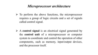
- 4. Microprocessor architecture ➢ Microprocessor architecture refers to the internal structure and organization of components in a microprocessor, including its registers, buses, instruction set, and control unit, which collectively determine how it processes data. ➢ The function of microprocessor can be classified into three general categories; (i) Microprocessor-initiated operations (ii) internal operations (iii) peripheral operations.
- 5. Microprocessor architecture ➢ To perform the above functions, the microprocessor requires a group of logic circuits and a set of signals called control signal. ➢ A control signal is an electrical signal generated by the control unit of a microprocessor or computer system to coordinate and control the operation of other components, such as memory, input/output devices, and the processor itself.
- 6. Microprocessor architecture ➢ The Central Processing Unit (CPU) and the Micro Processor Unit (MPU) is related but not same. A CPU can be implemented as a combination of more than one chip. ➢ Whereas, the MPU refers a single chip processor. The microprocessor and Micro Processor Unit often are used synonymously.
- 7. Microprocessor initiated operations and Bus Organization
- 8. Microprocessor initiated operations ➢ Microprocessor-initiated operations are tasks performed by the microprocessor to communicate with memory and peripherals, such as memory read, memory write, I/O read, and I/O write operations. ➢ The MPU performs primarily four operations : 1. Memory Read : Reads data or instructions from memory. 2. Memory Write : Write data or instructions into memory. 3. I/O Read : Accepts data from input devices. 4. I/O Write : Sends data to output devices.
- 9. Microprocessor initiated operations ➢ To communicate with a peripheral or a memory location, the MPU needs to perform the following steps: 1. Identify the peripheral or the memory location (with its address) 2. Transfer binary information (data and instruction) 3. Provide timing or synchronization signals. The 8085 MPU performs these functions using three sets of communication lines called buses: the address bus, the data bus, and the control bus.
- 10. 8085 Bus Organization ➢ The 8085 bus organization refers to the system of buses used by the 8085 microprocessor to communicate with memory, input/output devices, and other components as shown in Figure 1.1. ➢ The 8085 microprocessor has three primary buses: Address Bus, Data Bus, and Control Bus, each serving a specific purpose in the microprocessor's operation.
- 11. 8085 Bus Organization Fig. 1.1 The 8085 Bus Structure
- 12. Address Bus ➢ The address bus is a group of 16 lines generally identified as A0 to A15. ➢ It is unidirectional (bits flow in one direction) from the microprocessor to the memory or peripheral devices. ➢ The MPU uses the address bus to specify the memory location or I/O device to be accessed. ➢ In the 8085 microprocessors, the address is 16 bits, allowing access to 216=65,536 (64 KB) memory locations.
- 13. Address Bus
- 14. Data Bus ➢ The data bus is a group of 8 lines generally identified as D0 to D7. ➢ It is bi-directional (bits flow in both direction) between the microprocessor and the memory or peripheral devices. ➢ The data bus is used to transfer data between the processor, memory, and I/O devices. ➢ The eight data lines enable the MPU to manipulate 8- bit data ranging from 00 to FF (28 =256).
- 15. Data Bus ➢ The smallest number that can appear on the data bus 0000 0000 (00). ➢ The largest number that can appear on the data bus 1111 1111 (FF). ➢ so that the 8085 is known as an 8-bit microprocessor
- 16. Difference between Data Bus and Address Bus S. No.Feature Data Bus Address Bus 1. Direction Bidirectional Unidirectional 2. Purpose Transfers data or instructions Carries memory/I/O addresses 3. Size (8085) 8 bits 16 bits 4 Functional ity Exchanges data between components Identifies memory or I/O locations
- 17. Control Bus ➢ The control bus is comprised of various single lines that carry synchronization signals. ➢ It is used to provide the timing or synchronization signals. ➢ The control bus lines are not a group of lines like address bus or data bus, the individual lines that provide a pulse to indicate an MPU operation. ➢ The MPU generates control signals for every operation (such as memory read or memory write operations).
- 18. Control Bus ➢ The control bus carries control signals to coordinate and manage communication between the processor, memory, and peripherals. Important control signals include: o RD (Read): Indicates data is being read. o WR (Write): Indicates data is being written. o ALE (Address Latch Enable): Distinguishes address and data on the same lines. o IO/M: Differentiates memory and I/O operations. The control bus ensures proper synchronization during data transfer.
- 19. Control Bus - Example ➢ For Example the following instruction, the data 78 is transferred into Register B. 2000 06 MVI B,78H ➢ Here 2000 is a memory location, 06 is a hex code for immediate data transfer to Register B. Fig. 1.2 Memory Read Operation
- 20. Control Bus - Example ➢ The following sequence of steps to be followed to read an instruction from a memory location as shown in Fig 1.2. 1. 16 -bit address (2000) placed on the address bus. 2. The address is decoded by external logic circuit and the memory location is identified. 3. MPU sends the memory read control signal (pulse). 4. The pulse activates the memory chip. 5. The contents of the memory location (8-bit data – 06) placed on the data bus and brought inside the MPU.
- 21. Internal Data Operations and the 8085 Registers
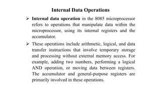
- 22. Internal Data Operations ➢ Internal data operation in the 8085 microprocessor refers to operations that manipulate data within the microprocessor, using its internal registers and the accumulator. ➢ These operations include arithmetic, logical, and data transfer instructions that involve temporary storage and processing without external memory access. For example, adding two numbers, performing a logical AND operation, or moving data between registers. The accumulator and general-purpose registers are primarily involved in these operations.
- 23. Internal Data Operations ➢ The internal architecture of the 8085 microprocessor determines how and what operations can be performed with the data. These operations are ➢ Store 8-bit data ➢ Perform arithmetic and logical operations. ➢ Test for conditions (Carry Flag). ➢ Sequence the execution of instructions (Program Counter) ➢ Store data temporarily during execution in the defined R/W memory locations called the stack.
- 24. 8085 Registers ➢ To perform the above operations, the microprocessor requires registers, an arithmetic/logic unit (ALU) , control logic and internal buses. ➢ The programming model of the 8085 displaying the internal registers and accumulator as shown in the figure 1.3. Fig. 1.3 The 8085 Programmable Registers
- 25. 8085 Registers ➢ The 8085 microprocessor has several programmable registers that perform specific functions in data handling and processing. ➢ Here's a concise explanation of each component: ➢ Accumulator (A): Stores results of arithmetic, logical operations, and intermediate data. ➢ General Purpose Registers (B, C, D, E, H, L): Used for temporary storage of data during operations. ➢ Flag Register: Contains status flags (Z, S, P, CY, AC) indicating conditions after operations.
- 26. 8085 Registers ➢ Program Counter (PC): Holds the address of the next instruction to be executed. ➢ Stack Pointer (SP): Points to the top of the stack, used for subroutine calls and returns. ➢ Instruction Register (IR): Holds the current instruction being decoded and executed. ➢ Temporary Register: Holds intermediate data during execution, typically used for internal operations.
- 27. Microprocessor function - Example program ➢ The following example program (addition of two numbers) demonstrates the function of the microprocessor. ➢ The hex codes of the program are stored in memory locations from 2000 to 2005 as shown in Fig. 1.2.
- 28. Microprocessor function with Example program Memory Location Hex Code Mnemonics Comments 2000 06 MVI B, 78H ; Transfer the value 78 into Register B. 2001 78 2002 3E MVI A, F2H ; Transfer the value F2 to Accumulator. 2003 F2 2004 80 ADD B ; The content of Register B is added with Accumulator and the results are stored in Accumulator. 2005 76 HLT ; Terminate the Program
- 29. Microprocessor function with Example program ➢ When executes the above instructions, the microprocessor places the address 2000 into address bus and increments the address in the PC (Program Counter) to 2001 for the next operation. It brings the code 06, interprets the code, places the address 2001 on the address bus, and then gets byte 78H and increments the address in PC to 2002. ➢ The First two instruction is used to transfer the data into register B and Register A.
- 30. Microprocessor function with Example program ➢ The third instruction ADD is used to perform the addition operation and the result is stored into accumulator. In this case 78 + F2 = 16AH, the accumulator holds only the value 6A, the value 1 indicates the carry flag. ➢ The Fourth instruction terminates the program.
- 31. Peripheral or Externally Initiated Operation ➢ External devices can initiate the following operations : Reset, Interrupt, Ready and Hold. ➢ Reset : When the reset pin is activated by external key (reset key), all internal operations are suspended and the program counter is cleared. Now, the program execution can begin at the zero memory address. ➢ Interrupt : The microprocessor can be interrupted from the normal execution of instructions and asked to execute some other instructions called a service routine. The microprocessor resumes its operation after completing the service routine.
- 32. Peripheral or Externally Initiated Operation ➢ Ready : If the signal of this ready pin is low, the microprocessor enters into a wait state.If it is high, the microprocessor ready to send or receive data. ➢ Hold : When the HOLD pin is activated by an external signal, the microprocessor relinquishes control of buses and allows the external peripherals to use them. For example, the HOLD signal is used in Direct Memory Access (DMA) data transfer.
- 33. Difference between Microprocessor-initiated operation and Peripheral-Initiated Operation Feature Microprocessor-Initiated Peripheral-Initiated Initiator Microprocessor External device (peripheral) Examples Memory Read, Memory Write, I/O Read Interrupts, Direct Memory Access (DMA) Control Controlled by microprocessor signals Triggered by external signals Priority Sequentially executed Can interrupt current operations Execution Part of the microprocessor program flow Requires special handling like ISR