MICROPROCESSOR & MICROCONTROLLER 8086,8051 Notes
70 likes18,193 views

The document provides information about a microprocessor and microcontroller course. It includes details about the 8086 microprocessor such as its architecture, registers, buses, instruction set, and flag register. It discusses the 8086's internal architecture which consists of a bus interface unit and execution unit. The execution unit decodes and executes instructions, and contains components like the ALU, general purpose registers, and flag register. The document also provides a brief history of microprocessor development from early 4-bit and 8-bit processors to modern 64-bit processors.


![8086 Microprocessor-introduction
INTEL launched 8086 in 1978
8086 is a 16-bit microprocessor with
• 16-bit Data Bus {D0-D15}
• 20-bit Address Bus {A0-A19} [can access upto
2^20= 1 MB memory locations] .
It has multiplexed address and data bus
AD0-AD15 and A16–A19.
It can support upto 64K I/O ports
46](https://image.slidesharecdn.com/ec6504-mpmcall5unitsfinal-150515171614-lva1-app6891/85/MICROPROCESSOR-MICROCONTROLLER-8086-8051-Notes-46-320.jpg)


![3. DIRECT ADDRESSING MODE
• Memory address is supplied with in
the instruction
• Mnemonic: MOV AH,[MEMBDS]
AH [1000H]
• But the memory address is not
index or pointer register
79](https://image.slidesharecdn.com/ec6504-mpmcall5unitsfinal-150515171614-lva1-app6891/85/MICROPROCESSOR-MICROCONTROLLER-8086-8051-Notes-79-320.jpg)
![4. REGISTER INDIRECT ADDRESSING MODE
• Memory address is supplied in an index or
pointer register
• EX:
MOV AX,[SI] ; AL [SI] ; AH [SI+1]
JMP [DI] ; IP [DI+1: DI]
INC BYTE PTR [BP] ; [BP] [BP]+1
DEC WORD PTR [BX] ;
[BX+1:BX] [BX+1:BX]-1
80](https://image.slidesharecdn.com/ec6504-mpmcall5unitsfinal-150515171614-lva1-app6891/85/MICROPROCESSOR-MICROCONTROLLER-8086-8051-Notes-80-320.jpg)
![5.Indexed Addressing Mode
• Memory address is the sum of index
register plus displacement
MOV AX,[SI+2] AL [SI+2]; AH [SI+3]
JMP [DI+2] IP [BX+3:BX+2]
81](https://image.slidesharecdn.com/ec6504-mpmcall5unitsfinal-150515171614-lva1-app6891/85/MICROPROCESSOR-MICROCONTROLLER-8086-8051-Notes-81-320.jpg)
![6. Based Addressing Mode
• Memory address is the sum of the BX or BP
base register plus a displacement within
instruction
• Ex:
MOV AX,[BP+2] AL [BP+2]; AH [BP+3]
JMP [BX+2] IP [BX+3:BX+2]
82](https://image.slidesharecdn.com/ec6504-mpmcall5unitsfinal-150515171614-lva1-app6891/85/MICROPROCESSOR-MICROCONTROLLER-8086-8051-Notes-82-320.jpg)
![7.BASED & INDEX ADDRESSING MODES
• Memory address is the sum of the index register
& base register
Ex:
MOV AX,[BX+SI] ; AL [BX+SI] ; AH [BX+SI+1]
JMP [BX+DI] ; IP [BX+DI+1 : BX+DI]
INC BYTE PTR [BP+SI] ; [BP] [BP]+1
DEC WORD PTR [BP+DI] ;
[BX+1:BX] [BX+1:BX]-1
83](https://image.slidesharecdn.com/ec6504-mpmcall5unitsfinal-150515171614-lva1-app6891/85/MICROPROCESSOR-MICROCONTROLLER-8086-8051-Notes-83-320.jpg)
![8. BASED & INDEXED WITH DISPLACEMENT ADDRESSING MODE
• Memory address is the sum of an index register ,
base register and displacement within instruction
MOV AX,[BX+SI+6] ; AL [BX+SI+6] ; AH [BX+SI+7]
JMP [BX+DI+6] ; IP [BX+DI+7 : BX+DI+6]
INC BYTE PTR [BP+SI+5] ;
DEC WORD PTR [BP+DI+5] ;
84Presented by C.GOKUL,AP/EEE , Velalar College of Engg & Tech, Erode](https://image.slidesharecdn.com/ec6504-mpmcall5unitsfinal-150515171614-lva1-app6891/85/MICROPROCESSOR-MICROCONTROLLER-8086-8051-Notes-84-320.jpg)
![9. Strings Addressing Mode
• The memory source address is a register SI in the
data segment, and the memory destination
address is register DI in the extra segment
• Ex: MOVSB [ES:DI] [DS:SI]
• If DF=0 SI SI+1 , DI DI+1
DF=1 SI SI-1 , DI DI-1
85](https://image.slidesharecdn.com/ec6504-mpmcall5unitsfinal-150515171614-lva1-app6891/85/MICROPROCESSOR-MICROCONTROLLER-8086-8051-Notes-85-320.jpg)


![(1). Data copy/transfer instructions.
(1). MOV Destination, Source
There will be transfer of data from source to destination.
Source can be register, memory location or immediate
data.
Destination can be register or memory operand.
Both Source and Destination cannot be memory location
or segment registers at the same time.
E.g.
(1). MOV CX, 037A H;
(2). MOV AL, BL;
(3). MOV BX, [0301 H];
90](https://image.slidesharecdn.com/ec6504-mpmcall5unitsfinal-150515171614-lva1-app6891/85/MICROPROCESSOR-MICROCONTROLLER-8086-8051-Notes-90-320.jpg)


![(2). Push Source
Source can be register, segment register or
memory.
This instruction pushes the contents of specified
source on to the stack.
In this stack pointer is decremented by 2.
The higher byte data is pushed first (SP-1).
Then lower byte data is pushed (SP-2).
E.g.:
(1). PUSH AX;
(2). PUSH DS;
(3). PUSH [5000H];
93](https://image.slidesharecdn.com/ec6504-mpmcall5unitsfinal-150515171614-lva1-app6891/85/MICROPROCESSOR-MICROCONTROLLER-8086-8051-Notes-93-320.jpg)


![(3) POP Destination
Destination can be register, segment register or
memory.
This instruction pops (takes) the contents of
specified destination.
In this stack pointer is incremented by 2.
The lower byte data is popped first (SP+1).
Then higher byte data is popped (SP+2).
E.g.
(1). POP AX;
(2). POP DS;
(3). POP [5000H];
96](https://image.slidesharecdn.com/ec6504-mpmcall5unitsfinal-150515171614-lva1-app6891/85/MICROPROCESSOR-MICROCONTROLLER-8086-8051-Notes-96-320.jpg)


![(4). XCHG Destination, source;
•This instruction exchanges contents of Source with
destination.
• It cannot exchange two memory locations directly.
•The contents of AL are exchanged with BL.
•The contents of AH are exchanged with BH.
•E.g.
(1). XCHG BX,AX;
(2). XCHG [5000H],AX;
99](https://image.slidesharecdn.com/ec6504-mpmcall5unitsfinal-150515171614-lva1-app6891/85/MICROPROCESSOR-MICROCONTROLLER-8086-8051-Notes-99-320.jpg)


![8.LEA 16-bit register (source), address (dest.)
LEA Also known as Load Effective Address
(LEA).
It loads effective address formed by the
destination into the source register.
E.g.
(1). LEA BX,Address;
(2). LEA SI,Address[BX];
106](https://image.slidesharecdn.com/ec6504-mpmcall5unitsfinal-150515171614-lva1-app6891/85/MICROPROCESSOR-MICROCONTROLLER-8086-8051-Notes-106-320.jpg)


![(3) INC source
This instruction increases the contents of source
operand by 1.
The source may be memory location or register.
The source can not be immediate data.
The result is stored in the same place.
E.g. (1). INC AX;
(2). INC [5000H];
115](https://image.slidesharecdn.com/ec6504-mpmcall5unitsfinal-150515171614-lva1-app6891/85/MICROPROCESSOR-MICROCONTROLLER-8086-8051-Notes-115-320.jpg)
![AFTER EXECUTION
5000H
AFTER EXECUTIONBEFORE EXECUTION
INC [5000H]
BEFORE EXECUTION
INC AXAH 10 AL 11 AH 10 AL 12
1011 5000H 1012
116](https://image.slidesharecdn.com/ec6504-mpmcall5unitsfinal-150515171614-lva1-app6891/85/MICROPROCESSOR-MICROCONTROLLER-8086-8051-Notes-116-320.jpg)
![4. DEC source
This instruction decreases the contents of
source operand by 1.
The source may be memory location or register.
The source can not be immediate data.
The result is stored in the same place.
E.g. (1). DEC AX;
(2). DEC [5000H];
117](https://image.slidesharecdn.com/ec6504-mpmcall5unitsfinal-150515171614-lva1-app6891/85/MICROPROCESSOR-MICROCONTROLLER-8086-8051-Notes-117-320.jpg)
![AFTER EXECUTION
5000H
AFTER EXECUTIONBEFORE EXECUTION
DEC [5000H]
BEFORE EXECUTION
DEC AXAH 10 AL 11 AH 10 AL 10
1051 5000H 1050
118](https://image.slidesharecdn.com/ec6504-mpmcall5unitsfinal-150515171614-lva1-app6891/85/MICROPROCESSOR-MICROCONTROLLER-8086-8051-Notes-118-320.jpg)


![SUM of N numbers
MOV AX,0000
MOV SI,1100
MOV DI,1200
MOV CX,0005 5 NUMBERS TO BE TAKEN SUM
MOV DX,0000
L1: ADD AX,[SI]
INC SI
INC DX
CMP CX,DX
JNZ L1
MOV [1200],AX
HLT 199](https://image.slidesharecdn.com/ec6504-mpmcall5unitsfinal-150515171614-lva1-app6891/85/MICROPROCESSOR-MICROCONTROLLER-8086-8051-Notes-199-320.jpg)
![Average of N numbers
MOV AX,0000
MOV SI,1100
MOV DI,1200
MOV CX,0005 5 NUMBERS TO BE TAKEN AVERAGE
MOV DX,0000
L1: ADD AX,[SI]
INC SI
INC DX
CMP CX,DX
JNZ L1
DIV CX AX=AX/5(AVERAGE OF 5 NUMBERS)
MOV [1200],AX
HLT 200Presented by C.GOKUL,AP/EEE , Velalar College of Engg & Tech, Erode](https://image.slidesharecdn.com/ec6504-mpmcall5unitsfinal-150515171614-lva1-app6891/85/MICROPROCESSOR-MICROCONTROLLER-8086-8051-Notes-200-320.jpg)
![FACTORIAL of N
MOV CX,0005 5 Factorial=5*4*3*2*1=120
MOV DX,0000
MOV AX,0001
L1: MUL CX
DEC DX
CMP CX,DX
JNZ L1
MOV [1200],AX
HLT
201](https://image.slidesharecdn.com/ec6504-mpmcall5unitsfinal-150515171614-lva1-app6891/85/MICROPROCESSOR-MICROCONTROLLER-8086-8051-Notes-201-320.jpg)


![• Macros are just like procedures, but not really.
• Macros exist only until your code is compiled
• After compilation all macros are replaced with
real instructions
• several macros to make coding easier(Reduce
large & complex programs)
Example (Macro definition)
name MACRO [parameters,...]
<instructions>
ENDM
228](https://image.slidesharecdn.com/ec6504-mpmcall5unitsfinal-150515171614-lva1-app6891/85/MICROPROCESSOR-MICROCONTROLLER-8086-8051-Notes-228-320.jpg)


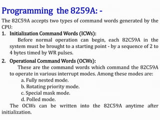
![Type – 0 Divide Error Interrupt
Quotient is too large cant be fit in AL/AX or Divide By Zero {AX/0=∞}
Type –1 Single Step Interrupt
used for executing the program in single step mode by setting Trap Flag
To Set Trap Flag PUSHF
MOV BP,SP
OR [BP+0],0100H;SET BIT8
POPF
Type – 2 Non Maskable Interrupt
This Interrupt is used for executing ISR of NMI Pin (Positive Egde Signal). NMI
cant be masked by S/W
Type – 3 Break Point Interrupt
used for providing BREAK POINTS in the program
Type – 4 Over Flow Interrupt
used to handle any Overflow Error after signed arithmetic
244](https://image.slidesharecdn.com/ec6504-mpmcall5unitsfinal-150515171614-lva1-app6891/85/MICROPROCESSOR-MICROCONTROLLER-8086-8051-Notes-244-320.jpg)


![Byte Manipulation
Example 1:
MOV AX,[1000]
MOV BX,[1002]
AND AX,BX
MOV [2000],AX
HLT
Example 2:
MOV AX,[1000]
MOV BX,[1002]
OR AX,BX
MOV [2000],AX
HLT
Example 3:
MOV AX,[1000]
MOV BX,[1002]
XOR AX,BX
MOV [2000],AX
HLT
Example 4:
MOV AX,[1000]
NOT AX
MOV [2000],AX
HLT
248
Presented by C.GOKUL,AP/EEE , Velalar College of Engg & Tech, Erode](https://image.slidesharecdn.com/ec6504-mpmcall5unitsfinal-150515171614-lva1-app6891/85/MICROPROCESSOR-MICROCONTROLLER-8086-8051-Notes-248-320.jpg)


![8086 ALP:
1100: START: MOV BX, 1200H
MOV CX, 0008H
MOV AL,[BX]
MOV DX, CONTROL PORT
OUT DX, AL
INC BX
NEXT: MOV AL,[BX]
MOV DX, PORT A
OUT DX,AL
CALL DELAY
INC BX
LOOP NEXT
JMP START
DELAY: PUSH CX
MOV CX,0005H
REPEAT: MOV DX,0FFFFH
LOOP2: DEC DX
JNZ LOOP2
LOOP REPEAT
POP CX
RET
467](https://image.slidesharecdn.com/ec6504-mpmcall5unitsfinal-150515171614-lva1-app6891/85/MICROPROCESSOR-MICROCONTROLLER-8086-8051-Notes-467-320.jpg)


![Special
Function
Registers [SFR]
520](https://image.slidesharecdn.com/ec6504-mpmcall5unitsfinal-150515171614-lva1-app6891/85/MICROPROCESSOR-MICROCONTROLLER-8086-8051-Notes-520-320.jpg)


![Program Status Word [PSW]
C AC F0 RS1 RS0 OV F1 P
Register Bank Select
Carry
Auxiliary Carry
User Flag 0
Parity
User Flag 1
Overflow
523
00-Bank 0
01-Bank 1
10-Bank 2
11-Bank 3](https://image.slidesharecdn.com/ec6504-mpmcall5unitsfinal-150515171614-lva1-app6891/85/MICROPROCESSOR-MICROCONTROLLER-8086-8051-Notes-523-320.jpg)


MICROPROCESSOR & MICROCONTROLLER 8086,8051 Notes
- 1. Presented by C.GOKUL,AP/EEE Velalar College of Engg & Tech, Erode Email: [email protected] EC6504 Microprocessor & Microcontroller DEPARTMENTS: ECE {semester 05} CSE,IT {semester 04} Regulation : 2013 ANNA UNIVERSITY Syllabus
- 2. syllabus 2
- 3. 3
- 4. BOOK References Main Book: 1. Microprocessors and Interfacing, Programming and Hardware by Doughlas V.Hall Other Authors: 2. Microcomputer Systems: The 8086 / 8088 Family - Architecture, Programming and Design by Yu-Cheng Liu, Glenn A.Gibson 3. INTEL Microprocessors 8086/8088, 80186/80188, 80286, 80386, 80486, Pentium, Prentium ProProcessor, Pentium II, III, 4 by Barry B. Bery 4. Advanced microprocessor and peripherals by A K RAY LOCAL AUTHOR: 8086 Microprocessor by Nagoor Kani => Unit 1,2,3 8051 Microcontroller by V Udayashankara => Unit 4,5 4
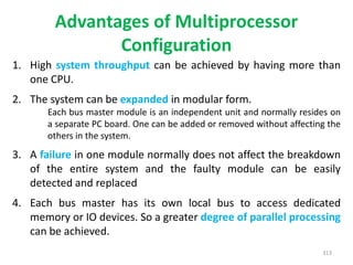
- 5. NPTEL Lecture Materials References • Microprocessor and Peripheral Devices by Dr. Pramod Agarwal , IIT Roorkee Link: http://nptel.ac.in/courses/108107029/ • Microprocessors and Microcontrollers by Prof. Krishna Kumar IISc Bangalore Link: http://nptel.ac.in/courses/106108100/ 5
- 6. Microprocessor Basics • Microprocessor (µP) is the “brain” of a computer that has been implemented on one semiconductor chip. • The word comes from the combination micro and processor. • Processor means a device that processes whatever(binary numbers, 0’s and 1’s) To process means to manipulate. It describes all manipulation. Micro - > extremely small 6
- 7. Definition of a Microprocessor. The microprocessor is a programmable device that takes in numbers, performs on them arithmetic or logical operations according to the program stored in memory and then produces other numbers as a result. 7
- 8. Microprocessor ? A microprocessor is multi programmable clock driven register based semiconductor device that is used to fetch , process & execute a data within fraction of seconds. 8
- 9. Applications • Calculators • Accounting system • Games machine • Instrumentation • Traffic light Control • Multi user, multi-function environments • Military applications • Communication systems 9
- 11. DIFFERENT PROCESSORS AVAILABLE Socket Processor Pinless Processor Slot Processor ProcessorSl ot 11
- 12. Development of Intel Microprocessors • 8086 - 1979 • 286 - 1982 • 386 - 1985 • 486 - 1989 • Pentium - 1993 • Pentium Pro - 1995 • Pentium MMX -1997 • Pentium II - 1997 • Pentium II Celeron - 1998 • Pentium II Zeon - 1998 • Pentium III - 1999 • Pentium III Zeon - 1999 • Pentium IV - 2000 • Pentium IV Zeon - 2001 12
- 13. GENERATION OF PROCESSORS Processor Bits Speed 8080 8 2 MHz 8086 16 4.5 – 10 MHz 8088 16 4.5 – 10 MHz 80286 16 10 – 20 MHz 80386 32 20 – 40 MHz 80486 32 40 – 133 MHz 13
- 14. GENERATION OF PROCESSORS Processor Bits Speed Pentium 32 60 – 233 MHz Pentium Pro 32 150 – 200 MHz Pentium II, Celeron , Xeon 32 233 – 450 MHz Pentium III, Celeron , Xeon 32 450 MHz – 1.4 GHz Pentium IV, Celeron , Xeon 32 1.3 GHz – 3.8 GHz Itanium 64 800 MHz – 3.0 GHz 14
- 15. Intel 4004 Introduced in 1971. It was the first microprocessor by Intel. It was a 4-bit µP. Its clock speed was 740KHz. It had 2,300 transistors. It could execute around 60,000 instructions per second. 15
- 16. Intel 4040 Introduced in 1971. It was also 4-bit µP. 16
- 18. Intel 8008 Introduced in 1972. It was first 8-bit µP. Its clock speed was 500 KHz. Could execute 50,000 instructions per second. 18
- 19. Intel 8080 Introduced in 1974. It was also 8-bit µP. Its clock speed was 2 MHz. It had 6,000 transistors. 19
- 20. Intel 8085 Introduced in 1976. It was also 8-bit µP. Its clock speed was 3 MHz. Its data bus is 8-bit and address bus is 16-bit. It had 6,500 transistors. Could execute 7,69,230 instructions per second. It could access 64 KB of memory. It had 246 instructions. 20
- 22. INTEL 8086 Introduced in 1978. It was first 16-bit µP. Its clock speed is 4.77 MHz, 8 MHz and 10 MHz, depending on the version. Its data bus is 16-bit and address bus is 20-bit. It had 29,000 transistors. Could execute 2.5 million instructions per second. It could access 1 MB of memory. It had 22,000 instructions. It had Multiply and Divide instructions. 22
- 23. INTEL 8088 Introduced in 1979. It was also 16-bit µP. It was created as a cheaper version of Intel’s 8086. It was a 16-bit processor with an 8-bit external bus. 23
- 24. INTEL 80186 & 80188 Introduced in 1982. They were 16-bit µPs. Clock speed was 6 MHz. 80188 was a cheaper version of 80186 with an 8-bit external data bus. 24
- 25. INTEL 80286 Introduced in 1982. It was 16-bit µP. Its clock speed was 8 MHz. Its data bus is 16-bit and address bus is 24- bit. It could address 16 MB of memory. It had 1,34,000 transistors. 25
- 27. INTEL 80386 Introduced in 1986. It was first 32-bit µP. Its data bus is 32-bit and address bus is 32- bit. It could address 4 GB of memory. It had 2,75,000 transistors. Its clock speed varied from 16 MHz to 33 MHz depending upon the various versions. 27
- 28. INTEL 80486 Introduced in 1989. It was also 32-bit µP. It had 1.2 million transistors. Its clock speed varied from 16 MHz to 100 MHz depending upon the various versions. 8 KB of cache memory was introduced. 28
- 29. INTEL PENTIUM Introduced in 1993. It was also 32-bit µP. It was originally named 80586. Its clock speed was 66 MHz. Its data bus is 32-bit and address bus is 32- bit. 29
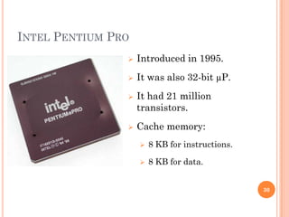
- 30. INTEL PENTIUM PRO Introduced in 1995. It was also 32-bit µP. It had 21 million transistors. Cache memory: 8 KB for instructions. 8 KB for data. 30
- 31. INTEL PENTIUM II Introduced in 1997. It was also 32-bit µP. Its clock speed was 233 MHz to 500 MHz. Could execute 333 million instructions per second. 31
- 32. INTEL PENTIUM II XEON Introduced in 1998. It was also 32-bit µP. It was designed for servers. Its clock speed was 400 MHz to 450 MHz. 32
- 33. INTEL PENTIUM III Introduced in 1999. It was also 32-bit µP. Its clock speed varied from 500 MHz to 1.4 GHz. It had 9.5 million transistors. 33
- 34. INTEL PENTIUM IV Introduced in 2000. It was also 32-bit µP. Its clock speed was from 1.3 GHz to 3.8 GHz. It had 42 million transistors. 34
- 35. INTEL DUAL CORE Introduced in 2006. It is 32-bit or 64-bit µP. 35
- 36. 36
- 38. Intel Core 2 Intel Core i3 38
- 39. INTEL CORE I5 INTEL CORE I7 39
- 40. Basic Terms • Bit: A digit of the binary number { 0 or 1 } • Nibble: 4 bit Byte: 8 bit word: 16 bit • Double word: 32 bit • Data: binary number/code operated by an instruction • Address: Identification number for memory locations • Clock: square wave used to synchronize various devices in µP • Memory Capacity = 2^n , n->no. of address lines 40
- 41. BUS CONCEPT • BUS: Group of conducting lines that carries data , address & control signals. CLASSIFICATION OF BUSES: 1.DATA BUS: group of conducting lines that carries data. 2. ADDRESS BUS: group of conducting lines that carries address. 3.CONTROL BUS: group of conducting lines that carries control signals {RD, WR etc} CPU BUS: group of conducting lines that directly connected to µP SYSTEM BUS: group of conducting lines that carries data , address & control signals in a µP system 41
- 42. TRISTATE LOGIC 3 logic levels are: • High State (logic 1) • Low state (logic 0) • High Impedance state High Impedance: output is not being driven to any defined logic level by the output circuit. 42
- 43. Basic Microprocessors System Input Devices Processing Data into Information Output Devices Control Unit Secondary Storage Devices Arithmetic- Logic Unit Primary Storage Unit Central Processing Unit Keyboard, Mouse etc Monitor Printer Disks, Tapes, Optical Disks 43
- 45. UNIT 1 Syllabus • Introduction to 8086 • Microprocessor architecture • Addressing modes • Instruction set • Assembler directives • Assembly language programming • Modular Programming 1.Linking and Relocation 2.Stacks , Procedures , Macros • Interrupts and interrupt service routines • Byte & String Manipulation. 45
- 46. 8086 Microprocessor-introduction INTEL launched 8086 in 1978 8086 is a 16-bit microprocessor with • 16-bit Data Bus {D0-D15} • 20-bit Address Bus {A0-A19} [can access upto 2^20= 1 MB memory locations] . It has multiplexed address and data bus AD0-AD15 and A16–A19. It can support upto 64K I/O ports 46
- 47. 8086 Microprocessor It provides 14, 16-bit registers. 8086 requires one phase clock with a 33% duty cycle to provide optimized internal timing. – Range of clock: • 5 MHz for 8086 • 8Mhz for 8086-2 • 10Mhz for 8086-1 47
- 48. 8086 Internal Architecture 8086 employs parallel processing 8086 CPU has two parts which operate at the same time • Bus Interface Unit • Execution Unit CPU functions 1. Fetch 2. Decode 3. Execute 8086 CPU Bus Interface Unit (BIU) Execution Unit (EU) 48
- 49. Bus Interface Unit Sends out addresses for memory locations Fetches Instructions from memory Reads/Writes data to memory Sends out addresses for I/O ports Reads/Writes data to Input/Output ports 49
- 50. Execution Unit Tells BIU (addresses) where to fetch instructions or data Decodes & Executes instructions Dividing the work between BIU & EU speeds up processing 50
- 51. Architecture Diagram of 8086 51
- 52. AH AL BH BL CH CL DH DL STACK POINTER (SP) BASE POINTER (BP) SOURCE INDEX (SI) DESTINATION INDEX (DI) EXTRA SEGMENT (ES) CODE SEGMENT (CS) STACK SEGMENT (SS) DATA SEGMENT (DS) INSTRUCTION POINTER (IP) 6 5 4 3 2 1 CONTROL SYSTEM ARITHMETIC LOGIC UNIT FLAGS Instruction Queue OPERANDS ∑ Memory Interface EU BIU Instruction Decoder 52
- 53. Execution Unit Main components are • Instruction Decoder • Control System • Arithmetic Logic Unit • General Purpose Registers • Flag Register • Pointer & Index registers 53
- 54. Instruction Decoder Translates instructions fetched from memory into a series of actions which EU carries out Control System Generates timing and control signals to perform the internal operations of the microprocessor Arithmetic Logic Unit EU has a 16-bit ALU which can ADD, SUBTRACT, AND, OR, increment, decrement, complement or shift binary numbers 54
- 55. General Purpose Registers EU has 8 general purpose registers Can be individually used for storing 8-bit data AL register is also called Accumulator Two registers can also be combined to form 16-bit registers The valid register pairs are – AX, BX, CX, DX AH AL BH BL CH CL DH DL AH AL AX BH BL BX CH CL CX DH DL DX 55
- 56. Flag Register 8086 has a 16-bit flag register Contains 9 active flags There are two types of flags in 8086 • Conditional flags – six flags, set or reset by EU on the basis of results of some arithmetic operations • Control flags – three flags, used to control certain operations of the processor 56
- 57. U U U U OF DF IF TF SF ZF U AF U PF U CF Flag Register 1. CF CARRY FLAG Conditional Flags (Compatible with 8085, except OF) 2. PF PARITY FLAG 3. AF AUXILIARY CARRY 4. ZF ZERO FLAG 5. SF SIGN FLAG 6. OF OVERFLOW FLAG 7. TF TRAP FLAG Control Flags 8. IF INTERRUPT FLAG 9. DF DIRECTION FLAG 57
- 58. Flag Register 58 15 14 13 12 11 10 9 8 7 6 5 4 3 2 1 0 OF DF IF TF SF ZF AF PF CF Carry Flag This flag is set, when there is a carry out of MSB in case of addition or a borrow in case of subtraction. Parity Flag This flag is set to 1, if the lower byte of the result contains even number of 1’s ; for odd number of 1’s set to zero. Auxiliary Carry Flag This is set, if there is a carry from the lowest nibble, i.e, bit three during addition, or borrow for the lowest nibble, i.e, bit three, during subtraction. Zero Flag This flag is set, if the result of the computation or comparison performed by an instruction is zero Sign Flag This flag is set, when the result of any computation is negative Tarp Flag If this flag is set, the processor enters the single step execution mode by generating internal interrupts after the execution of each instruction Interrupt Flag Causes the 8086 to recognize external mask interrupts; clearing IF disables these interrupts. Direction Flag This is used by string manipulation instructions. If this flag bit is ‘0’, the string is processed beginning from the lowest address to the highest address, i.e., auto incrementing mode. Otherwise, the string is processed from the highest address towards the lowest address, i.e., auto incrementing mode. Over flow Flag This flag is set, if an overflow occurs, i.e, if the result of a signed operation is large enough to accommodate in a destination register. The result is of more than 7-bits in size in case of 8-bit signed operation and more than 15-bits in size in case of 16-bit sign operations, then the overflow will be set.
- 59. 59 Registers, Flag Sl.No. Type Register width Name of register 1 General purpose register 16 bit AX, BX, CX, DX 8 bit AL, AH, BL, BH, CL, CH, DL, DH 2 Pointer register 16 bit SP, BP 3 Index register 16 bit SI, DI 4 Instruction Pointer 16 bit IP 5 Segment register 16 bit CS, DS, SS, ES 6 Flag (PSW) 16 bit Flag register 8086 registers categorized into 4 groups 15 14 13 12 11 10 9 8 7 6 5 4 3 2 1 0 OF DF IF TF SF ZF AF PF CF
- 60. 60 Register Name of the Register Special Function AX 16-bit Accumulator Stores the 16-bit results of arithmetic and logic operations AL 8-bit Accumulator Stores the 8-bit results of arithmetic and logic operations BX Base register Used to hold base value in base addressing mode to access memory data CX Count Register Used to hold the count value in SHIFT, ROTATE and LOOP instructions DX Data Register Used to hold data for multiplication and division operations SP Stack Pointer Used to hold the offset address of top stack memory BP Base Pointer Used to hold the base value in base addressing using SS register to access data from stack memory SI Source Index Used to hold index value of source operand (data) for string instructions DI Data Index Used to hold the index value of destination operand (data) for string operations Registers and Special Functions
- 61. Bus Interface Unit Main Components are • Instruction Queue • Segment Registers • Instruction Pointer 61
- 62. Instruction Queue 8086 employs parallel processing When EU is busy decoding or executing current instruction, the buses of 8086 may not be in use. At that time, BIU can use buses to fetch upto six instruction bytes for the following instructions BIU stores these pre-fetched bytes in a FIFO register called Instruction Queue When EU is ready for its next instruction, it simply reads the instruction from the queue in BIU 62
- 63. Pipelining EU of 8086 does not have to wait in between for BIU to fetch next instruction byte from memory So the presence of a queue in 8086 speeds up the processing Fetching the next instruction while the current instruction executes is called pipelining 63
- 64. Memory Segmentation 8086 has a 20-bit address bus So it can address a maximum of 1MB of memory 8086 can work with only four 64KB segments at a time within this 1MB range These four memory segments are called • Code segment • Stack segment • Data segment • Extra segment 64
- 65. 1 2 3 4 5 6 7 8 9 10 11 12 13 14 15 16 Memory 00000H FFFFFH 1MB Address Range 64KB Memory Segment Only 4 such segments can be addressed at a time 4 5 6 7 65
- 66. Code Segment That part of memory from where BIU is currently fetching instruction code bytes Stack Segment A section of memory set aside to store addresses and data while a subprogram executes Data & Extra Segments Used for storing data values to be used in the program 66
- 67. 1 2 3 4 5 6 7 8 9 10 11 12 13 14 15 16 Memory 00000H FFFFFH 1MB Address Range Code Segment Stack Segment Data & Extra Segments 67
- 68. Segment Registers hold the upper 16-bits of the starting address for each of the segments The four segment registers are • CS (Code Segment register) • DS (Data Segment register) • SS (Stack Segment register) • ES (Extra Segment register) 68
- 69. 1 Code Segment 3 4 Data Segment Extra Segment 7 8 9 10 11 12 13 14 15 Stack Segment Memory 00000H FFFFFH 1MB Address Range StartingAddresses ofSegments 1000 0H 4000 0H 5000 0H F000 0H CS DS ES SS 69
- 70. Address of a segment is of 20-bits A segment register stores only upper 16- bits BIU always inserts zeros for the lowest 4- bits of the 20-bit starting address. E.g. if CS = 348AH, then the code segment will start at 348A0H A 64-KB segment can be located anywhere in the memory, but will start at an address with zeros in the lowest 4-bits 70
- 71. Instruction Pointer (IP) Register a 16-bit register Holds 16-bit offset, of the next instruction byte in the code segment BIU uses IP and CS registers to generate the 20-bit address of the instruction to be fetched from memory 71
- 72. 1 Data Segment 3 4 Code Segment Extra Segment 7 8 9 10 11 12 13 14 15 Stack Segment Memory 00000H FFFFFH 1MB Address Range 348A H 4214 H 38AB4 H CS IP Physical Address Start of Code Segment 348A0H Code Byte MOV AL, BL38AB4H IP = 4214H + 0 Physical Address Calculation 72
- 73. Stack Segment (SS) Register Stack Pointer (SP) Register Upper 16-bits of the starting address of stack segment is stored in SS register It is located in BIU SP register holds a 16-bit offset from the start of stack segment to the top of the stack It is located in EU 73
- 74. Other Pointer & Index Registers Base Pointer (BP) register Source Index (SI) register Destination Index (DI) register Can be used for temporary storage of data Main use is to hold a 16-bit offset of a data word in one of the segments 74
- 76. Various Addressing Modes 1. Immediate Addressing Mode 2. Register Addressing Mode 3. Direct Addressing Mode 4. Register Indirect Addressing Mode 5. Index Addressing Mode 6. Based Addressing Mode 7. Based & Indexed Addressing Mode 8. Based & Indexed with displacement Addressing Mode 9. Strings Addressing Mode 76 Presented by C.GOKUL,AP/EEE , Velalar College of Engg & Tech, Erode
- 77. 1. IMMEDIATE ADDRESSING MODE • The instruction will specify the name of the register which holds the data to be operated by the instruction. • Source data is within the instruction • Ex: MOV AX,10ABH AL=ABH, AH=10H 77
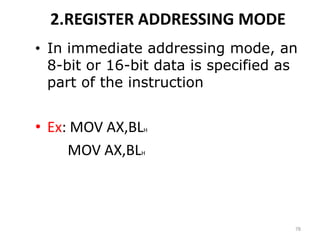
- 78. 2.REGISTER ADDRESSING MODE • In immediate addressing mode, an 8-bit or 16-bit data is specified as part of the instruction • Ex: MOV AX,BLH MOV AX,BLH 78
- 79. 3. DIRECT ADDRESSING MODE • Memory address is supplied with in the instruction • Mnemonic: MOV AH,[MEMBDS] AH [1000H] • But the memory address is not index or pointer register 79
- 80. 4. REGISTER INDIRECT ADDRESSING MODE • Memory address is supplied in an index or pointer register • EX: MOV AX,[SI] ; AL [SI] ; AH [SI+1] JMP [DI] ; IP [DI+1: DI] INC BYTE PTR [BP] ; [BP] [BP]+1 DEC WORD PTR [BX] ; [BX+1:BX] [BX+1:BX]-1 80
- 81. 5.Indexed Addressing Mode • Memory address is the sum of index register plus displacement MOV AX,[SI+2] AL [SI+2]; AH [SI+3] JMP [DI+2] IP [BX+3:BX+2] 81
- 82. 6. Based Addressing Mode • Memory address is the sum of the BX or BP base register plus a displacement within instruction • Ex: MOV AX,[BP+2] AL [BP+2]; AH [BP+3] JMP [BX+2] IP [BX+3:BX+2] 82
- 83. 7.BASED & INDEX ADDRESSING MODES • Memory address is the sum of the index register & base register Ex: MOV AX,[BX+SI] ; AL [BX+SI] ; AH [BX+SI+1] JMP [BX+DI] ; IP [BX+DI+1 : BX+DI] INC BYTE PTR [BP+SI] ; [BP] [BP]+1 DEC WORD PTR [BP+DI] ; [BX+1:BX] [BX+1:BX]-1 83
- 84. 8. BASED & INDEXED WITH DISPLACEMENT ADDRESSING MODE • Memory address is the sum of an index register , base register and displacement within instruction MOV AX,[BX+SI+6] ; AL [BX+SI+6] ; AH [BX+SI+7] JMP [BX+DI+6] ; IP [BX+DI+7 : BX+DI+6] INC BYTE PTR [BP+SI+5] ; DEC WORD PTR [BP+DI+5] ; 84Presented by C.GOKUL,AP/EEE , Velalar College of Engg & Tech, Erode
- 85. 9. Strings Addressing Mode • The memory source address is a register SI in the data segment, and the memory destination address is register DI in the extra segment • Ex: MOVSB [ES:DI] [DS:SI] • If DF=0 SI SI+1 , DI DI+1 DF=1 SI SI-1 , DI DI-1 85
- 87. • Instruction:- An instruction is a binary pattern designed inside a microprocessor to perform a specific function. • Opcode:- It stands for operational code. It specifies the type of operation to be performed by CPU. It is the first field in the machine language instruction format. • E.g. 08 is the opcode for instruction “MOV X,Y”. • Operand:- We can also say it as data on which operation should act. operands may be register values or memory values. The CPU executes the instructions using information present in this field. It may be 8-bit data or 16-bit data. Instruction set basics 87
- 88. • Assembler:- it converts the instruction into sequence of binary bits, so that this bits can be read by the processor. • Mnemonics:- these are the symbolic codes for either instructions or commands to perform a particular function. • E.g. MOV, ADD, SUB etc. Instruction set basics 88
- 89. Types of instruction set of 8086 microprocessor (1). Data Copy/Transfer instructions. (2).Arithmetic & Logical instructions. (3). Branch instructions. (4). Loop instructions. (5). Machine Control instructions. (6). Flag Manipulation instructions. (7). Shift & Rotate instructions. (8). String instructions. 89
- 90. (1). Data copy/transfer instructions. (1). MOV Destination, Source There will be transfer of data from source to destination. Source can be register, memory location or immediate data. Destination can be register or memory operand. Both Source and Destination cannot be memory location or segment registers at the same time. E.g. (1). MOV CX, 037A H; (2). MOV AL, BL; (3). MOV BX, [0301 H]; 90
- 91. BX 2000HAX 2000H BEFORE EXECUTION AFTER EXECUTION MOV BX,AX A H AL B H BL C H CL D H DL A H AL B H BL C H CL 40 D H DL MOV CL,M 40 40 BEFORE EXECUTION AFTER EXECUTION 91
- 92. Stack Pointer It is a 16-bit register, contains the address of the data item currently on top of the stack. Stack operation includes pushing (providing) data on to the stack and popping (taking)data from the stack. Pushing operation decrements stack pointer and Popping operation increments stack pointer. i.e. there is a last in first out (LIFO) operation. 92
- 93. (2). Push Source Source can be register, segment register or memory. This instruction pushes the contents of specified source on to the stack. In this stack pointer is decremented by 2. The higher byte data is pushed first (SP-1). Then lower byte data is pushed (SP-2). E.g.: (1). PUSH AX; (2). PUSH DS; (3). PUSH [5000H]; 93
- 94. INITIAL POSITION DECREMENTS SP & STORES HIGHER BYTE HIGHER BYTE DECREMENTS SP & STORES LOWER BYTE LOWER BYTE HIGHER BYTE (1) STACK POINTER (2) STACK POINTER (3) STACK POINTER 94
- 95. BH BL CH 10 CL 50 DH DL BH BL CH 10 CL 50 DH DL 50 10 SP 2002H SP 2000H BEFORE EXECUTION AFTER EXECUTION 2000H 2001H 2002H 2000H 2001H 2002H PUSH CX 95
- 96. (3) POP Destination Destination can be register, segment register or memory. This instruction pops (takes) the contents of specified destination. In this stack pointer is incremented by 2. The lower byte data is popped first (SP+1). Then higher byte data is popped (SP+2). E.g. (1). POP AX; (2). POP DS; (3). POP [5000H]; 96
- 97. INITIAL POSITION AND READS LOWER BYTE LOWER BYTE INCREMENTS SP & READS HIGHER BYTE LOWER BYTE HIGHER BYTE INCREMENTS SP LOWER BYTE HIGHER BYTE (1) STACK POINTER (2) STACK POINTER (3) STACK POINTER 97
- 98. BH BL BH 5 0 BL 30 SP 2000H SP 2002H 30 50 30 50 BEFORE EXECUTION AFTER EXECUTION POP BX 2000H 2001H 2002H 2000H 2001H 2002H 98
- 99. (4). XCHG Destination, source; •This instruction exchanges contents of Source with destination. • It cannot exchange two memory locations directly. •The contents of AL are exchanged with BL. •The contents of AH are exchanged with BH. •E.g. (1). XCHG BX,AX; (2). XCHG [5000H],AX; 99
- 100. AH 20 AL 40 BH 70 BL 80 AH 70 AL 80 BH 20 BL 40 BEFORE EXECUTION AFTER EXECUTION XCHG AX,BX 100
- 101. (5)IN AL/AX, 8-bit/16-bit port address It reads from the specified port address. It copies data to accumulator from a port with 8- bit or 16-bit address. DX is the only register is allowed to carry port address. E.g. (1). IN AL, 80H; (2). IN AX,DX; //DX contains address of 16-bit port. 101
- 102. 10 AL 10 AL 10 BEFORE EXECUTION AFTER EXECUTION IN AL,80H PORT 80H PORT 80H 102
- 103. OUT 8-bit/16-bit port address,AL/AX It writes to the specified port address. It copies contents of accumulator to the port with 8-bit or 16-bit address. DX is the only register is allowed to carry port address. E.g. (1). OUT 80H,AL; (2). OUT DX,AX; //DX contains address of 16-bit port. 103
- 104. 10 AL 40 40 AL 40 BEFORE EXECUTION AFTER EXECUTION OUT 50H,AL PORT 50H PORT 50H 104
- 105. (7) XLAT Also known as translate instruction. It is used to find out codes in case of code conversion. i.e. it translates code of the key pressed to the corresponding 7-segment code. After execution this instruction contents of AL register always gets replaced. E.g. XLAT; 105
- 106. 8.LEA 16-bit register (source), address (dest.) LEA Also known as Load Effective Address (LEA). It loads effective address formed by the destination into the source register. E.g. (1). LEA BX,Address; (2). LEA SI,Address[BX]; 106
- 107. (9). LDS 16-bit register (source), address (dest.); (10). LES 16-bit register (source), address (dest.); LDS Also known as Load Data Segment (LDS). LES Also known as Load Extra Segment (LES). It loads the contents of DS (Data Segment) or ES (Extra Segment) & contents of the destination to the contents of source register. E.g. (1). LDS BX,5000H; (2). LES BX,5000H; 107
- 108. 10 20 30 40 5000H 5001H 5002H 5003H 20 10 40 30 (1). LDS BX,5000H; (2). LES BX,5000H; BX DS/ES 07015 108
- 109. (11). LAHF:- This instruction loads the AH register from the contents of lower byte of the flag register. This command is used to observe the status of the all conditional flags of flag register. E.g. LAHF; (12). SAHF:- This instruction sets or resets all conditional flags of flag register with respect to the corresponding bit positions. If bit position in AH is 1 then related flag is set otherwise flag will be reset. E.g. SAHF; 109
- 110. PUSH & POP (13). PUSH F:- This instruction decrements the stack pointer by 2. It copies contents of flag register to the memory location pointed by stack pointer. E.g. PUSH F; (14). POP F:- This instruction increments the stack pointer by 2. It copies contents of memory location pointed by stack pointer to the flag register. E.g. POP F; 110
- 111. (2).Arithmetic Instructions These instructions perform the operations like: Addition, Subtraction, Increment, Decrement. 111
- 112. (2).Arithmetic Instructions (1).ADD destination, source; This instruction adds the contents of source operand with the contents of destination operand. The source may be immediate data, memory location or register. The destination may be memory location or register. The result is stored in destination operand. AX is the default destination register. E.g. (1).ADD AX,2020H; (2).ADD AX,BX; 112
- 113. AH 10 AL 10 AFTER EXECUTION BEFORE EXECUTION AH 10 AL 10 BH 20 BL 20 AFTER EXECUTIONBEFORE EXECUTION ADD AX,2020H ADD AX,BX AH 30 AL 30 1010 +2020 3030 AH 30 AL 30 BH 20 BL 20 113
- 114. ADC destination, source This instruction adds the contents of source operand with the contents of destination operand with carry flag bit. The source may be immediate data, memory location or register. The destination may be memory location or register. The result is stored in destination operand. AX is the default destination register. E.g. (1).ADC AX,2020H; (2).ADC AX,BX; 114
- 115. (3) INC source This instruction increases the contents of source operand by 1. The source may be memory location or register. The source can not be immediate data. The result is stored in the same place. E.g. (1). INC AX; (2). INC [5000H]; 115
- 116. AFTER EXECUTION 5000H AFTER EXECUTIONBEFORE EXECUTION INC [5000H] BEFORE EXECUTION INC AXAH 10 AL 11 AH 10 AL 12 1011 5000H 1012 116
- 117. 4. DEC source This instruction decreases the contents of source operand by 1. The source may be memory location or register. The source can not be immediate data. The result is stored in the same place. E.g. (1). DEC AX; (2). DEC [5000H]; 117
- 118. AFTER EXECUTION 5000H AFTER EXECUTIONBEFORE EXECUTION DEC [5000H] BEFORE EXECUTION DEC AXAH 10 AL 11 AH 10 AL 10 1051 5000H 1050 118
- 119. (5) SUB destination, source; This instruction subtracts the contents of source operand from contents of destination. The source may be immediate data, memory location or register. The destination may be memory location or register. The result is stored in the destination place. E.g. (1). SUB AX,1000H; (2). SUB AX,BX; 119
- 120. AFTER EXECUTIONBEFORE EXECUTION SUB AX,1000H AFTER EXECUTIONBEFORE EXECUTION SUB AX,BX AH 20 AL 00 AH 10 AL 00 2000 -1000 =1000 AH 20 AL 00 BH 10 BL 00 AH 10 AL 00 BH 10 BL 00 120
- 121. (6). SBB destination, source; Also known as Subtract with Borrow. This instruction subtracts the contents of source operand & borrow from contents of destination operand. The source may be immediate data, memory location or register. The destination may be memory location or register. The result is stored in the destination place. E.g. (1). SBB AX,1000H; (2). SBB AX,BX; 121
- 122. AH 20 AL 20 AFTER EXECUTIONBEFORE EXECUTION AH 20 AL 20 BH 10 BL 10 AFTER EXECUTIONBEFORE EXECUTION SBB AX,1000H SBB AX,BX 2050 AH 10 AL 19 2020 - 1000 1020- 1=1019 AH 10 AL 19 BH 10 BL 10 B 1 B 1 122
- 123. (7). CMP destination, source Also known as Compare. This instruction compares the contents of source operand with the contents of destination operands. The source may be immediate data, memory location or register. The destination may be memory location or register. Then resulting carry & zero flag will be set or reset. E.g. (1). CMP AX,1000H; (2). CMP AX,BX; 123
- 124. AFTER EXECUTION CMP AX,BX BEFORE EXECUTION CY 0 Z 1 AFTER EXECUTIONBEFORE EXECUTION D=S: CY=0,Z=1 D>S: CY=0,Z=0 D<S: CY=1,Z=0 AH 10 AL 00 BH 10 BL 00 CMP AX,BX CY 0 Z 0 AH 10 AL 00 BH 00 BL 10 AFTER EXECUTIONBEFORE EXECUTION CMP AX,BX CY 1 Z 0 AH 10 AL 00 BH 20 BL 00 124
- 125. AAA (ASCII Adjust after Addition): The data entered from the terminal is inASCII format. InASCII, 0 – 9 are represented by 30H – 39H. This instruction allows us to add theASCII codes. This instruction does not have any operand. Other ASCII Instructions: AAS (ASCIIAdjust after Subtraction) AAM (ASCIIAdjust after Multiplication) AAD (ASCIIAdjust Before Division) 125
- 126. DAA (Decimal Adjust after Addition) It is used to make sure that the result of adding two BCD numbers is adjusted to be a correct BCD number. It only works onAL register. DAS (Decimal Adjust after Subtraction) It is used to make sure that the result of subtracting two BCD numbers is adjusted to be a correct BCD number. It only works onAL register. 126
- 127. MUL operand Unsigned Multiplication. Operand contents are positively signed. Operand may be general purpose register or memory location. If operand is of 8-bit then multiply it with contents of AL. If operand is of 16-bit then multiply it with contents of AX. Result is stored in accumulator (AX). E.g. (1). MUL BH // AX= AL*BH; // (+3) * (+4) = +12. (2). MUL CX // AX=AX*CX; 127
- 128. IMUL operand Signed Multiplication. Operand contents are negatively signed. Operand may be general purpose register, memory location or index register. If operand is of 8-bit then multiply it with contents of AL. If operand is of 16-bit then multiply it with contents of AX. Result is stored in accumulator (AX). E.g. (1). IMUL BH // AX= AL*BH; // (-3) * (-4) = 12. (2). IMUL CX // AX=AX*CX; 128
- 129. DIV operand Unsigned Division. Operand may be register or memory. Operand contents are positively signed. Operand may be general purpose register or memory location. AL=AX/Operand (8-bit/16-bit) & AH=Remainder. E.g. MOV AX, 0203 // AX=0203 MOV BL, 04 // BL=04 IDIV BL // AL=0203/04=50 (i.e.AL=50 & AH=03) 129
- 130. IDIV operand Signed Division. Operand may be register or memory. Operand contents are negatively signed. Operand may be general purpose register or memory location. AL=AX/Operand (8-bit/16-bit) & AH=Remainder. E.g. MOV AX, -0203 // AX=-0203 MOV BL, 04 // BL=04 DIV BL // AL=-0203/04=-50 (i.e.AL=-50 & AH=03) 130
- 131. Multiplication and Division Examples 131
- 132. AH 00 AL 05 BH 00 BL 03 CH CL 132 BEFORE EXECUTION AFTER EXECUTION MUL BX AX=lower 16 bit {000F} DX=Higher 16 bit {0000} AH 00 AL 0F BH BL CH CL DH 00 DL 00 0005*0003 = 0000 000F
- 133. AH 00 AL 0F BH 00 BL 02 CH CL 133 BEFORE EXECUTION AFTER EXECUTION DIV BX AH 00 AL 07 BH BL CH CL DH 00 DL 01 AX=Quotient {0007} DX=Reminder {0001} 000F = 7 1 0002 2
- 134. 134
- 135. 135
- 136. 136
- 137. LOGICAL (or) Bit Manipulation Instructions These instructions are used at the bit level. These instructions can be used for: Testing a zero bit Set or reset a bit Shift bits across registers 137
- 138. Bit Manipulation Instructions(LOGICAL Instructions) • AND – Especially used in clearing certain bits (masking) xxxx xxxx AND 0000 1111 = 0000 xxxx (clear the first four bits) – Examples: AND BL, 0FH • OR – Used in setting certain bits xxxx xxxx OR 0000 1111 = xxxx 1111 (Set the upper four bits) 138
- 139. XOR – Used in Inverting bits xxxx xxxx XOR 0000 1111 = xxxxx’x’x’x’ -Example: Clear bits 0 and 1, set bits 6 and 7, invert bit 5 of register CL: AND CL, FCH ; 1111 1100B OR CL, C0H ; 1100 0000B XOR CL, 20H ; 0010 0000B 139
- 140. 140 AFTER EXECUTION BEFORE EXECUTION AND AX,BXH AH 11 AL 11 BH 11 BL 11 AH FF AL FF BH 11 BL 11 AX = FFFFH = 1111 1111 1111 1111 BX = 1111H = 0001 0001 0001 0001 AND (&) AND 0001 0001 0001 0001 = 1111H
- 141. 141 AFTER EXECUTION BEFORE EXECUTION OR AX,BXH AH FF AL FF BH 11 BL 11 AH FF AL FF BH 11 BL 11 AX = FFFFH = 1111 1111 1111 1111 BX = 1111H = 0001 0001 0001 0001 OR OR 1111 1111 1111 1111 = FFFFH
- 142. 142 AFTER EXECUTION BEFORE EXECUTION XOR AX,BXH AH EE AL EE BH 11 BL 11 AH FF AL FF BH 11 BL 11 AX = FFFFH = 1111 1111 1111 1111 BX = 1111H = 0001 0001 0001 0001 XOR 1110 1110 1110 1110 = EEEEH
- 143. 143 AFTER EXECUTION BEFORE EXECUTION NOT AXH AH 00 AL 00AH FF AL FF AX = FFFFH = 1111 1111 1111 1111 NOT 0000 0000 0000 0000 = 0000H
- 144. SHL Instruction The SHL (shift left) instruction performs a logical left shift on the destination operand, filling the lowest bit with 0. CF 0 mov dl,5d shl dl,1 144
- 145. SHR Instruction The SHR (shift right) instruction performs a logical right shift on the destination operand.The highest bit position is filled with a zero. CF 0 MOV DL,80d SHR DL,1 ; DL = 40 SHR DL,2 ; DL = 10 145
- 146. SAR Instruction SAR (shift arithmetic right) performs a right arithmetic shift on the destination operand. CF An arithmetic shift preserves the number's sign. MOV DL,-80 SAR DL,1 ; DL = -40 SAR DL,2 ; DL = -10 146
- 147. mov dl,5 shl dl,1 Shifting left n bits multiplies the operand by 2n For example, 5 * 22 = 20 Shifting right n bits divides the operand by 2n For example, 80 / 23 = 10 0 0 0 0 1 0 1 0 0 0 0 0 0 1 0 1 = 5 = 10 Before: After: 147
- 148. ROL Instruction ROL (rotate) shifts each bit to the left The highest bit is copied into both the Carry flag and into the lowest bit No bits are lost CF MOV Al,11110000b ROL Al,1 ; AL = 11100001b MOV Dl,3Fh ROL Dl,4 ; DL = F3h 148
- 149. ROR Instruction ROR (rotate right) shifts each bit to the right The lowest bit is copied into both the Carry flag and into the highest bit No bits are lost CF MOV AL,11110000b ROR AL,1 ; AL = 01111000b MOV DL,3Fh ROR DL,4 ; DL = F3h 149
- 150. RCL Instruction RCL (rotate carry left) shifts each bit to the left Copies the Carry flag to the least significant bit Copies the most significant bit to the Carry flag CF CLC ; CF = 0 MOV BL,88H ; CF,BL = 0 10001000b RCL BL,1 ; CF,BL = 1 00010000b RCL BL,1 ; CF,BL = 0 00100001b 150
- 151. RCR Instruction RCR (rotate carry right) shifts each bit to the right Copies the Carry flag to the most significant bit Copies the least significant bit to the Carry flag STC ; CF = 1 MOV AH,10H ; CF,AH = 00010000 1 RCR AH,1 ; CF,AH = 10001000 0 CF 151
- 152. SHL Instruction The SHL (shift left) instruction performs a logical left shift on the destination operand, filling the lowest bit with 0. CF 0 152 0 0 0 0 0 1 0 1 =05H 0 0 0 0 1 0 1 0 CF 0 BEFORE EXECUTION AFTER EXECUTION =0AH
- 153. SHR Instruction 153 0 0 0 0 0 1 0 1 =05H 0 0 0 0 0 0 1 0 CF 1 CF 0 =02H BEFORE EXECUTION AFTER EXECUTION
- 154. ROL Instruction CF 154 0 0 0 0 0 1 0 1 =05H 0 0 0 0 1 0 1 0 CF 0 =0AH BEFORE EXECUTION AFTER EXECUTION
- 155. ROR Instruction CF 155 0 0 0 0 0 1 0 1 =05H 1 0 0 0 0 0 1 0 CF 1 =82H BEFORE EXECUTION AFTER EXECUTION
- 156. Branching Instructions (or) Program Execution Transfer Instructions These instructions cause change in the sequence of the execution of instruction. This change can be through a condition or sometimes unconditional. The conditions are represented by flags. 156
- 157. CALL Des: This instruction is used to call a subroutine or function or procedure. The address of next instruction after CALL is saved onto stack. RET: It returns the control from procedure to calling program. Every CALL instruction should have a RET. 157
- 158. SUBROUTINE & SUBROUTINE HANDILING INSTRUCTIONS Call subroutine A Next instruction Call subroutine A Next instruction Main program Subroutine A First Instruction Return 158
- 159. JMP Des: This instruction is used for unconditional jump from one place to another. Jxx Des (Conditional Jump): All the conditional jumps follow some conditional statements or any instruction that affects the flag. 159
- 160. Conditional Jump Table Mnemonic Meaning JA Jump ifAbove JAE Jump ifAbove or Equal JB Jump if Below JBE Jump if Below or Equal JC Jump if Carry JE Jump if Equal JNC Jump if Not Carry JNE Jump if Not Equal JNZ Jump if Not Zero JPE Jump if Parity Even JPO Jump if Parity Odd JZ Jump if Zero 160
- 161. Loop Des: This is a looping instruction. The number of times looping is required is placed in the CX register. With each iteration, the contents of CX are decremented. ZF is checked whether to loop again or not. 161
- 162. String Instructions String in assembly language is just a sequentially stored bytes or words. There are very strong set of string instructions in 8086. By using these string instructions, the size of the program is considerably reduced. 162
- 163. CMPS Des, Src: It compares the string bytes or words. SCAS String: It scans a string. It compares the String with byte in AL or with word in AX. 163
- 164. MOVS / MOVSB / MOVSW: It causes moving of byte or word from one string to another. In this instruction, the source string is in Data Segment and destination string is in Extra Segment. SI and DI store the offset values for source and destination index. 164
- 165. 1. Copying a string (MOV SB) MOV CX,0003 copy 3 memory locations MOV SI,1000 MOV DI,2000 L1 CLD MOV SB DEC CX decrement CX JNZ L1 HLT 165
- 166. 2. Find & Replace 166
- 167. REP (Repeat): This is an instruction prefix. It causes the repetition of the instruction until CX becomes zero. E.g.: REP MOVSB STR1, STR2 It copies byte by byte contents. REP repeats the operation MOVSB until CX becomes zero. 167
- 168. Processor Control Instructions These instructions control the processor itself. 8086 allows to control certain control flags that: causes the processing in a certain direction processor synchronization if more than one microprocessor attached. 168
- 169. STC It sets the carry flag to 1. CLC It clears the carry flag to 0. CMC It complements the carry flag. 169
- 170. STD: It sets the direction flag to 1. If it is set, string bytes are accessed from higher memory address to lower memory address. CLD: It clears the direction flag to 0. If it is reset, the string bytes are accessed from lower memory address to higher memory address. 170
- 171. HLT instruction – HALT processing The HLT instruction will cause the 8086 to stop fetching and executing instructions. NOP instruction this instruction simply takes up three clock cycles and does no processing. LOCK instruction this is a prefix to an instruction. This prefix makes sure that during execution of the instruction, control of system bus is not taken by other microprocessor. WAIT instruction this instruction takes 8086 to an idle condition. The CPU will not do any processing during this. 171
- 172. INSTRUCTION SET-summary 1.DATA TRANSFER INSTRUCTIONS Mnemonic Meaning Format Operation MOV Move Mov D,S (S) (D) XCHG Exchange XCHG D,S (S) (D) LEA Load Effective Address LEA Reg16,EA EA (Reg16) PUSH pushes the operand into top of stack. PUSH BX sp=sp-2 Copy 16 bit value to top of stack POP pops the operand from top of stack to Des. POP BX Copy top of stack to 16 bit reg sp=sp+2 IN transfers the operand from specified port to accumulator register. IN AL,28 OUT transfers the operand from accumulator to specified port. OUT 28,AL 172
- 173. 2. ARITHMETIC INSTRUCTIONS Mnemonic Meaning Format Operation SUB Subtract SUB D,S (D) - (S) (D) Borrow (CF) SBB Subtract with borrow SBB D,S (D) - (S) - (CF) (D) DEC Decrement by one DEC D (D) - 1 (D) NEG Negate NEG D DAS Decimal adjust for subtraction DAS Convert the result in AL to packed decimal format AAS ASCII adjust for subtraction AAS (AL) difference (AH) dec by 1 if borrow ADD Addition ADD D,S (S)+(D) (D) carry (CF) ADC Add with carry ADC D,S (S)+(D)+(CF) (D) carry (CF) INC Increment by one INC D (D)+1 (D) AAA ASCII adjust for addition AAA If the sum is >9, AH is incremented by 1 DAA Decimal adjust for addition DAA Adjust AL for decimal Packed BCD173
- 174. Mnemonic Meaning Format Operation AND OR XOR NOT Logical AND Logical Inclusive OR Logical Exclusive OR LOGICAL NOT AND D,S OR D,S XOR D,S NOT D (S) · (D) → (D) (S)+(D) → (D) (S) (D)→(D) (D) → (D) + 3. Bit Manipulation Instructions(Logical Instructions) 174 Presented by C.GOKUL,AP/EEE , Velalar College of Engg & Tech, Erode
- 175. Shift & Rotate Instructions Mnemonic Meaning Format ROL Rotate Left ROL D,Count ROR Rotate Right ROR D,Count RCL Rotate Left through Carry RCL D,Count RCR Rotate right through Carry RCR D,Count Mnemonic Meaning Format SAL/SHL SHR SAR Shift arithmetic Left/ Shift Logical left Shift logical right Shift arithmetic right SAL/SHL D, Count SHR D, Count SAR D, Count 175
- 176. 4. Branching or PROGRAM EXECUTION TRANSFER INSTRUCTIONS • CALL - call a subroutine • RET - returns the control from procedure to calling program • JMP Des – Unconditional Jump • Jxx Des – conditional Jump (ex: JC 8000) • Loop Des 176
- 177. 5. STRING INSTRUCTIONS • CMPS Des, Src - compares the string bytes • SCAS String - scans a string • MOVS / MOVSB / MOVSW - moving of byte or word • REP (Repeat) - repetition of the instruction 177
- 178. 6. PROCESSOR CONTROL INSTRUCTIONS • STC – set the carry flag (CF=1) • CLC – clear the carry flag (CF=0) • STD – set the direction flag (DF=1) • CLD – clear the direction flag (DF=0) • HLT – stop fetching & execution • NOP – no operation(no processing) • LOCK - control of system bus is not taken by other µP • WAIT - CPU will not do any processing • ESC - µP does NOP or access a data from memory for coprocessor 178
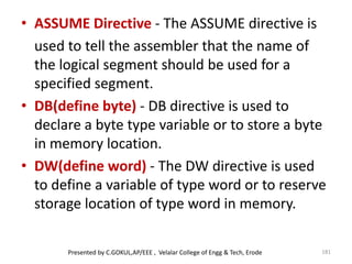
- 181. • ASSUME Directive - The ASSUME directive is used to tell the assembler that the name of the logical segment should be used for a specified segment. • DB(define byte) - DB directive is used to declare a byte type variable or to store a byte in memory location. • DW(define word) - The DW directive is used to define a variable of type word or to reserve storage location of type word in memory. 181Presented by C.GOKUL,AP/EEE , Velalar College of Engg & Tech, Erode
- 182. • DD(define double word) :This directive is used to declare a variable of type double word or restore memory locations which can be accessed as type double word. • DQ (define quadword) :This directive is used to tell the assembler to declare a variable 4 words in length or to reserve 4 words of storage in memory . • DT (define ten bytes):It is used to inform the assembler to define a variable which is 10 bytes in length or to reserve 10 bytes of storage in memory. 182
- 183. • END- End program .This directive indicates the assembler that this is the end of the program module. The assembler ignores any statements after an END directive. • ENDP- End procedure: It indicates the end of the procedure (subroutine) to the assembler. • ENDS-End Segment: This directive is used with the name of the segment to indicate the end of that logical segment. • EQU - This EQU directive is used to give a name to some value or to a symbol. 183
- 184. • PROC - The PROC directive is used to identify the start of a procedure. • PTR -This PTR operator is used to assign a specific type of a variable or to a label. • ORG -Originate : The ORG statement changes the starting offset address of the data. 184
- 185. Directives examples • ASSUME CS:CODE cs=> code segment • ORG 3000 • NAME DB ‘THOMAS’ • POINTER DD 12341234H • FACTOR EQU 03H 185
- 187. Program 1: Increment an 8-bit number • MOV AL, 05H Move 8-bit data to AL. • INC AL Increment AL. Program 2: Increment an 16-bit number • MOV AX, 0005H Move 16-bit data to AX. • INC AX Increment AX. 187Presented by C.GOKUL,AP/EEE , Velalar College of Engg & Tech, Erode After Execution AL = 06H After Execution AX = 0006H
- 188. Program 3: Decrement an 8-bit number • MOV AL, 05H Move 8-bit data to AL. • DEC AL Decrement AL. Program 4: Decrement an 16-bit number • MOV AX, 0005H Move 16-bit data to AX. • DEC AX Decrement AX. 188 After Execution AL = 04H After Execution AX = 0004H
- 189. Program 5: 1’s complement of an 8-bit number. • MOV AL, 05H Move 8-bit data to AL. • NOT AL Complement AL. Program 6: 1’s complement of a 16-bit number. • MOV AX, 0005H Move 16-bit data to AX. • NOT AX Complement AX. 189 After Execution AL = FAH After Execution AX = FFFAH
- 190. Program 7: 2’s complement of an 8-bit number. • MOV AL, 05H Move 8-bit data to AL. • NOT AL Complement AL. • INC AL Increment AL Program 8: 2’s complement of a 16-bit number. • MOV AX, 0005H Move 16-bit data to AX. • NOT AX Complement AX. • INC AX Increment AX 190 After Execution AX = FAH + 1 = FB After Execution AX = FFFAH + 1 = FFFB
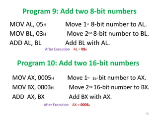
- 191. Program 9: Add two 8-bit numbers MOV AL, 05H Move 1st 8-bit number to AL. MOV BL, 03H Move 2nd 8-bit number to BL. ADD AL, BL Add BL with AL. Program 10: Add two 16-bit numbers MOV AX, 0005H Move 1st 16-bit number to AX. MOV BX, 0003H Move 2nd 16-bit number to BX. ADD AX, BX Add BX with AX. 191 After Execution AL = 08H After Execution AX = 0008H
- 192. Program 11: subtract two 8-bit numbers MOV AL, 05H Move 1st 8-bit number to AL. MOV BL, 03H Move 2nd 8-bit number to BL. SUB AL, BL subtract BL from AL. Program 12: subtract two 16-bit numbers MOV AX, 0005H Move 1st 16-bit number to AX. MOV BX, 0003H Move 2nd 16-bit number to BX. SUB AX, BX subtract BX from AX. 192 After Execution AL = 02H After Execution AX = 0002H
- 193. Program 13: Multiply two 8-bit unsigned numbers. MOV AL, 04H Move 1st 8-bit number to AL. MOV BL, 02H Move 2nd 8-bit number to BL. MUL BL Multiply BL with AL and the result will be in AX. Program 14: Multiply two 8-bit signed numbers. MOV AL, 04H Move 1st 8-bit number to AL. MOV BL, 02H Move 2nd 8-bit number to BL. IMUL BL Multiply BL with AL and the result will be in AX. 193
- 194. Program 15: Multiply two 16-bit unsigned numbers. MOV AX, 0004H Move 1st 16-bit number to AL. MOV BX, 0002H Move 2nd 16-bit number to BL. MUL BX Multiply BX with AX and the result will be in DX:AX {4*2=0008=> 08=> AX , 00=> DX} Program 16: Divide two 16-bit unsigned numbers. MOV AX, 0004H Move 1st 16-bit number to AL. MOV BX, 0002H Move 2nd 16-bit number to BL. DIV BX Divide BX from AX and the result will be in AX & DX {4/2=0002=> 02=> AX ,00=>DX} (ie: Quotient => AX , Reminder => DX ) 194Presented by C.GOKUL,AP/EEE , Velalar College of Engg & Tech, Erode
- 195. Detailed coding 16 BIT ADDITION 195
- 196. Detailed coding 16 BIT SUBTRACTION 196
- 198. 16 BIT DIVISION 198
- 199. SUM of N numbers MOV AX,0000 MOV SI,1100 MOV DI,1200 MOV CX,0005 5 NUMBERS TO BE TAKEN SUM MOV DX,0000 L1: ADD AX,[SI] INC SI INC DX CMP CX,DX JNZ L1 MOV [1200],AX HLT 199
- 200. Average of N numbers MOV AX,0000 MOV SI,1100 MOV DI,1200 MOV CX,0005 5 NUMBERS TO BE TAKEN AVERAGE MOV DX,0000 L1: ADD AX,[SI] INC SI INC DX CMP CX,DX JNZ L1 DIV CX AX=AX/5(AVERAGE OF 5 NUMBERS) MOV [1200],AX HLT 200Presented by C.GOKUL,AP/EEE , Velalar College of Engg & Tech, Erode
- 201. FACTORIAL of N MOV CX,0005 5 Factorial=5*4*3*2*1=120 MOV DX,0000 MOV AX,0001 L1: MUL CX DEC DX CMP CX,DX JNZ L1 MOV [1200],AX HLT 201
- 202. ASCENDING ORDER 202
- 203. 203
- 204. DECENDING ORDER Note: change the coding JNB L1 into JB L1 in the LINE 10 204
- 205. LARGEST, smallest NUMBER IN AN ARRAY 205
- 206. LARGEST NUMBER 206
- 207. SMALLEST NUMBER 207
- 209. • Generally , industry-programming projects consist of thousands of lines of instructions or operation code. • The size of the modules are reduced to a humanly comprehensible and manageable level. • Program is composed from several smaller modules. Modules could be developed by separate teams concurrently.OBJ modules (Object modules). • The .OBJ modules so produced are combined using a LINK program. • Modular programming techniques simplify the software development process 209
- 210. CHARACTERISTICS of module: 1. Each module is independent of other modules. 2. Each module has one input and one output. 3. A module is small in size. 4. Programming a single function per module is a goal Advantages of Modular Programming: • It is easy to write, test and debug a module. • Code can be reused. • The programmer can divide tasks. • Re-usable Modules can be re-used within a program DRAWBACKS: Modular programming requires extra time and memory 210
- 211. MODULAR PROGRAMMING: 1.LINKING & RELOCATION 2.STACKS 3.Procedures 4.Interrupts & Interrupt Routines 5.Macros 211
- 213. LINKER • A linker is a program used to join together several object files into one large object file. • The linker produces a link file which contains the binary codes for all the combined modules. The linker program is invoked using the following options. C> LINK or C>LINK MS.OBJ 213
- 214. • The loader is a part of the operating system and places codes into the memory after reading the ‘.exe’ file • A program called locator reallocates the linked file and creates a file for permanent location of codes in a standard format. 214
- 215. Creation and execution of a program 215
- 216. Loader ->Loader is a utility program which takes object code as input prepares it for execution and loads the executable code into the memory . ->Loader is actually responsible for initializing the process of execution. Functions of loaders: 1.It allocates the space for program in the memory(Allocation) 2.It resolves the code between the object modules(Linking) 3. some address dependent locations in the program, address constants must be adjusted according to allocated space(Relocation) 4. It also places all the machine instructions and data of corresponding programs and subroutines into the memory .(Loading) 216
- 217. Relocating loader (BSS Loader) • When a single subroutine is changed then all the subroutine needs to be reassembled. • The binary symbolic subroutine (BSS) loader used in IBM 7094 machine is relocating loader. • In BSS loader there are many procedure segments • The assembler reads one sourced program and assembles each procedure segment independently 217
- 218. • The output of the relocating loader is the object program • The assembler takes the source program as input; this source program may call some external routines. SEGMENT COMBINATION: ASM-86 assembler regulating the way segments with the same name are concatenated & sometimes they are overlaid. Form of segment directive: Segment name SEGEMENT Combine-type Possible combine-type are: • PUBLIC • COMMON • STACK • AT • MEMORY 218
- 219. Procedures 219 CALL & RET instruction
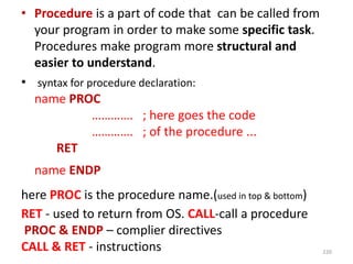
- 220. • Procedure is a part of code that can be called from your program in order to make some specific task. Procedures make program more structural and easier to understand. • syntax for procedure declaration: name PROC …………. ; here goes the code …………. ; of the procedure ... RET name ENDP here PROC is the procedure name.(used in top & bottom) RET - used to return from OS. CALL-call a procedure PROC & ENDP – complier directives CALL & RET - instructions 220
- 221. EXAMPLE 1 (call a procedure) ORG 100h CALL m1 MOV AX, 2 RET ; return to operating system. m1 PROC MOV BX, 5 RET ; return to caller. m1 ENDP END • The above example calls procedure m1, does MOV BX, 5 & returns to the next instruction after CALL: MOV AX, 2. 221Presented by C.GOKUL,AP/EEE , Velalar College of Engg & Tech, Erode
- 222. Example 2 : several ways to pass parameters to procedure ORG 100h MOV AL, 1 MOV BL, 2 CALL m2 CALL m2 CALL m2 CALL m2 RET ; return to operating system. m2 PROC MUL BL ; AX = AL * BL. RET ; return to caller. m2 ENDP END value of AL register is update every time the procedure is called. final result in AX register is 16 (or 10h)
- 223. 223 PUSH & POP instruction
- 224. • Stack is an area of memory for keeping temporary data. • STACK is used by CALL & RET instructions. PUSH -stores 16 bit value in the stack. POP -gets 16 bit value from the stack. • PUSH and POP instruction are especially useful because we don't have too much registers to operate 1. Store original value of the register in stack (using PUSH). 2. Use the register for any purpose. 3. Restore the original value of the register from stack (using POP). 224
- 225. Example-1 (store value in STACK using PUSH & POP) ORG 100h MOV AX, 1234h PUSH AX ; store value of AX in stack. MOV AX, 5678h ; modify the AX value. POP AX ; restore the original value of AX. RET END 225
- 226. Example 2: use of the stack is for exchanging the values ORG 100h MOV AX, 1212h ; store 1212h in AX. MOV BX, 3434h ; store 3434h in BX PUSH AX ; store value of AX in stack. PUSH BX ; store value of BX in stack. POP AX ; set AX to original value of BX. POP BX ; set BX to original value of AX. RET END push 1212h and then 3434h, on pop we will first get 3434h and only after it 1212h 226
- 227. MACROS 227 How to pass parameters using macros-6/8 Mark
- 228. • Macros are just like procedures, but not really. • Macros exist only until your code is compiled • After compilation all macros are replaced with real instructions • several macros to make coding easier(Reduce large & complex programs) Example (Macro definition) name MACRO [parameters,...] <instructions> ENDM 228
- 229. Example1 : Macro Definitions SAVE MACRO definition of MACRO name SAVE PUSH AX PUSH BX PUSH CX ENDM RETREIVE MACRO Another definition of MACRO name RETREIVE POP CX POP BX POP AX ENDM 229
- 230. 230
- 231. MACROS with Parameters Example: COPY MACRO x, y ; macro named COPY with 2 parameters{x, y} PUSH AX MOV AX, x MOV y, AX POP AX ENDM 231
- 233. INTERRUPT & ISR ? • ‘Interrupts’ is to break the sequence of operation. • While the CPU is executing a program, on ‘interrupt’ breaks the normal sequence of execution of instructions, diverts its execution to some other program called Interrupt Service Routine (ISR) 233
- 234. 234
- 235. 235
- 236. 236
- 237. • Maskable Interrupt: An Interrupt that can be disabled or ignored by the instructions of CPU are called as Maskable Interrupt. • Non- Maskable Interrupt: An interrupt that cannot be disabled or ignored by the instructions of CPU are called as Non- Maskable Interrupt. • Software interrupts are machine instructions that amount to a call to the designated interrupt subroutine, usually identified by interrupt number. Ex: INT0 - INT255 237
- 238. 238
- 239. 239
- 240. 240
- 241. 241
- 242. 242
- 243. INTERRUPT VECTOR TABLE 256 INTERRUPTS OF 8086 ARE DIVIDED IN TO 3 GROUPS 1. TYPE 0 TO TYPE 4 INTERRUPTS- These are used for fixed operations and hence are called dedicated interrupts 2. TYPE 5 TO TYPE 31 INTERRUPTS Not Used By 8086,reserved For Higher Processors Like 80286 80386 Etc 3. TYPE 32 TO 255 INTERRUPTS Available For User, called User Defined Interrupts These Can Be H/W Interrupts And Activated Through Intr Line Or Can Be S/W Interrupts. 243
- 244. Type – 0 Divide Error Interrupt Quotient is too large cant be fit in AL/AX or Divide By Zero {AX/0=∞} Type –1 Single Step Interrupt used for executing the program in single step mode by setting Trap Flag To Set Trap Flag PUSHF MOV BP,SP OR [BP+0],0100H;SET BIT8 POPF Type – 2 Non Maskable Interrupt This Interrupt is used for executing ISR of NMI Pin (Positive Egde Signal). NMI cant be masked by S/W Type – 3 Break Point Interrupt used for providing BREAK POINTS in the program Type – 4 Over Flow Interrupt used to handle any Overflow Error after signed arithmetic 244
- 245. PRIORITY OF INTERRUPTS Interrupt Type Priority INT0, INT3-INT 255, Highest NMI(INT2) INTR SINGLE STEP Lowest 245
- 247. Refer String Instructions in Instruction Set Slide No: 160-163 Move, compare, store, load, scan 247
- 248. Byte Manipulation Example 1: MOV AX,[1000] MOV BX,[1002] AND AX,BX MOV [2000],AX HLT Example 2: MOV AX,[1000] MOV BX,[1002] OR AX,BX MOV [2000],AX HLT Example 3: MOV AX,[1000] MOV BX,[1002] XOR AX,BX MOV [2000],AX HLT Example 4: MOV AX,[1000] NOT AX MOV [2000],AX HLT 248 Presented by C.GOKUL,AP/EEE , Velalar College of Engg & Tech, Erode
- 249. STRING MANIPULATION 1. Copying a string (MOV SB) MOV CX,0003 copy 3 memory locations MOV SI,1000 MOV DI,2000 L1 CLD MOV SB DEC CX decrement CX JNZ L1 HLT 249
- 250. 2. Find & Replace 250
- 251. UNIT-2 8086 SYSTEM BUS STRUCTURE 251 Presented by C.GOKUL,AP/EEE Velalar College of Engg & Tech , Erode DEPARTMENTS: CSE,IT {semester 04} ECE {semester 05} Regulation : 2013
- 252. UNIT 2 Syllabus 252
- 253. 8086 signals or Pin Diagram 253
- 254. INTEL 8086-Pin Diagram/Signal Description 254
- 255. INTEL 8086 - Pin Details Ground Clock Duty cycle: 33% Power Supply 5V ± 10% Reset Registers, seg regs, flags CS: FFFFH, IP: 0000H If high for minimum 4 clks 255
- 256. INTEL 8086 - Pin Details Address/Data Bus: Contains address bits A15-A0 when ALE is 1 & data bits D15 – D0 when ALE is 0. Address Latch Enable: When high, multiplexed address/data bus contains address information. 256
- 257. INTEL 8086 - Pin Details INTERRUPT Non - maskable interrupt Interrupt request Interrupt acknowledge 257
- 258. INTEL 8086 - Pin Details Direct Memory Access Hold acknowledge Hold 258
- 259. INTEL 8086 - Pin Details Address/Status Bus Address bits A19 – A16 & Status bits S6 – S3 259
- 260. INTEL 8086 - Pin Details Bus High Enable/S7 Enables most significant data bits D15 – D8 during read or write operation. S7: Always 1. BHE#, A0: 0,0: Whole word (16-bits) 0,1: High byte to/from odd address 1,0: Low byte to/from even address 1,1: No selection 260
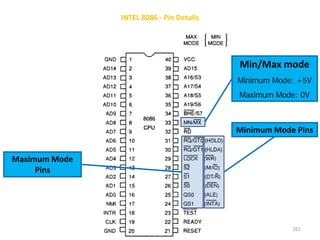
- 261. INTEL 8086 - Pin Details Min/Max mode Minimum Mode: +5V Maximum Mode: 0V Minimum Mode Pins Maximum Mode Pins 261
- 262. Minimum Mode- Pin Details Read Signal Write Signal Memory or I/0 Data Bus Enable Data Transmit/Receive 262
- 263. Maximum Mode - Pin Details Status Signal Inputs to 8288 to generate eliminated signals due to max mode. S2 S1 S0 000: INTA 001: read I/O port 010: write I/O port 011: halt 100: code access 101: read memory 110: write memory 111: none -passive 263
- 264. Maximum Mode - Pin Details DMA Request/Grant Lock Output Lock Output Used to lock peripherals off the system Activated by using the LOCK: prefix on any instruction 264
- 265. Maximum Mode - Pin Details Queue Status Used by numeric coprocessor (8087) QS1 QS0 00: Queue is idle 01: First byte of opcode 10: Queue is empty 11: Subsequent byte of opcode 265
- 266. GND AD14 AD13 AD12 AD11 AD10 AD9 AD8 AD7 AD6 AD5 AD4 AD3 AD2 AD1 AD0 NMI INTR CLK GND Vcc AD15 A16/S3 A17/S4 A18/S5 A19/S6___ BHE/S7 (HIGH)___ MN/MX___ RD ___ ____ HOLD (RQ/GT0)___ ____ HLDA (RQ/GT1)___ ______ WR (LOCK)__ __ IO/M (S2)__ __ DT/R (S1)____ __ DEN (S0) ALE (QS0)_____ INTA (QS1)_____ TEST READY RESET 1 40 INTEL 8086 20 21 Minmode operation signals (MN/MX=1) Maxmode operation signals (MN/MX=0) Time-multiplexed Address / Data Bus (bidirectional) Hardware interrupt requests (inputs) 2...5MHz, 1/3 duty cycle (input) 0V=“0”, reference for all voltages 5V±10% Time- multiplexed Address Bus /Status signals (outputs) Status signals (outputs) Operation Mode, (input): 1 = minmode (8088 generates all the needed control signals for a small system), 0 = maxmode (8288 Bus Controller expands the status signals to generate more control signals) Interrupt acknowledge (output) Control Bus (in,out) 266
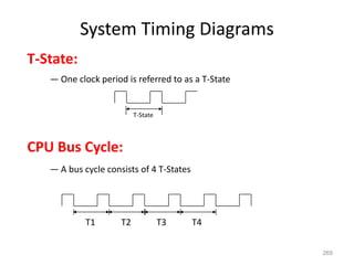
- 269. System Timing Diagrams T-State: — One clock period is referred to as a T-State T-State CPU Bus Cycle: — A bus cycle consists of 4 T-States T1 T2 T3 T4 269
- 270. Signal Transition occurs when the clock signal is HIGH Signal Transition occurs when the clock signal is LOW Signal Transition occurs from HIGH to LOW on RISING EDGE
- 271. AD0-AD15
- 277. Memory Read Timing Diagrams • Dump address on address bus. • Issue a read ( RD ) and set M/ IO to 1. • Wait for memory access cycle. 277
- 278. • Dump address on address bus. • Dump data on data bus. • Issue a write ( WR ) and set M/ IO to 1. Memory Write Timing Diagrams 278
- 279. Bus Timing During T 1 : • The address is placed on the Address/Data bus. • Control signals M/ IO , ALE and DT/ R specify memory or I/O, latch the address onto the address bus and set the direction of data transfer on data bus. During T 2 : • 8086 issues the RD or WR signal, DEN , and, for a write, the data. • DEN enables the memory or I/O device to receive the data for writes and the 8086 to receive the data for reads. During T 3 : • This cycle is provided to allow memory to access data. • READY is sampled at the end of T 2 . • If low, T 3 becomes a wait state. • Otherwise, the data bus is sampled at the end of T 3 . During T 4 : • All bus signals are deactivated, in preparation for next bus cycle. • Data is sampled for reads, writes occur for writes. 279
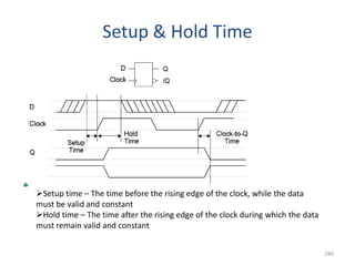
- 280. Setup & Hold Time Setup time – The time before the rising edge of the clock, while the data must be valid and constant Hold time – The time after the rising edge of the clock during which the data must remain valid and constant 280
- 281. WAIT State • A wait state (Tw) is an extra clocking period, inserted between T2 and T3, to lengthen the bus cycle, allowing slower memory and I/O components to respond. • The READY input is sampled at the end of T2, and again, if necessary in the middle of Tw. If READY is ‘0’ then a Tw is inserted. 1 2 3 4 Clock READY Tw 281
- 283. BASIC CONFIGURATIONS- 1.Minimum Mode 2.Maximum Mode – Minimum mode(MN/MX=Vcc) • Pin #33 (MN/MX) connect to +5V • Pin 24-31 are used as memory and I/O control signal • The control signals are generated internally by the 8086/88 • More cost-efficient – Maximum mode(MN/MX=GND) • Pin #33 (MN/MX) connect to Ground • Some control signals are generated externally by the 8288 bus controller chip • Max mode is used when math processor is used. 283
- 285. Minimum Mode 8086 System • 8086 is operated in minimum mode by MN/MX pin to logic 1 ( Vcc ). • In this mode, all the control signals are given out by the microprocessor chip itself. 285 NOTE: Explain Minimum mode signals also {refer pin diagram}
- 286. 286
- 288. 288
- 289. Memory READ in Minimum Mode
- 290. Memory WRITE in Minimum Mode
- 291. 2.Maximum Mode configuration NOTE: Explain Maximum mode signals also {refer pin diagram}
- 293. 8288 – BUS CONTROLLER 293
- 294. MAXIMUM MODE 294
- 295. 295
- 296. 296
- 299. Multiprocessor configuration • Multiprocessor Systems refer to the use of multiple processors that executes instructions simultaneously and communicate with each other using mail boxes and Semaphores. • Maximum mode of 8086 is designed to implement 3 basic multiprocessor configurations: 1. Coprocessor (8087) 2. Closely coupled (8089) 3. Loosely coupled (Multibus) 299
- 300. • Coprocessors and Closely coupled configurations are similar in that both the 8086 and the external processor shares the: - Memory - I/O system - Bus & bus control logic - Clock generator 300
- 301. Co-processor – Intel 8087 8087 instructions are inserted in the 8086 program 8086 and 8087 reads instruction bytes and puts them in the respective queues NOP 8087 instructions have 11011 as the MSB of their first code byte 301
- 302. Coprocessor / Closely Coupled Configuration 302
- 303. TEST pin of 8086 • Used in conjunction with the WAIT instruction in multiprocessing environments. • This is input from the 8087 coprocessor. • During execution of a wait instruction, the CPU checks this signal. • If it is low, execution of the signal will continue; if not, it will stop executing. 303
- 304. 1.Coprocessor Execution Example Coprocessor cannot take control of the bus, it does everything through the CPU 304
- 305. 2.Closely Coupled Execution Example • Closely Coupled processor may take control of the bus independently. • Two 8086’s cannot be closely coupled. 305
- 306. 3.Loosely Coupled Configuration • has shared system bus, system memory, and system I/O. • each processor has its own clock as well as its own memory (in addition to access to the system resources). • Used for medium to large multiprocessor systems. • Each module is capable of being the bus master. • Any module could be a processor capable of being a bus master, a coprocessor configuration or a closely coupled configuration. 306
- 307. 307
- 308. Loosely Coupled Configuration • No direct connections between the modules. • Each share the system bus and communicate through shared resources. • Processor in their separate modules can simultaneously access their private subsystems through their local busses, and perform their local data references and instruction fetches independently. This results in improved degree of concurrent processing. • Excellent for real time applications, as separate modules can be assigned specialized tasks 308
- 309. BUS ALLOCATION SCHEMES: Three bus allocation schemes: 1. Daisy Chaining 2. Pooling 3. Independent 1. Daisy Chaining: - Need a bus controller to monitor bus busy and bus request signals - Sends a bus grant to a Master >> each Master either keeps the service or passes it on - Controller synchronizes the clocks - Master releases the Bus Busy signal when finished
- 310. Daisy Chaining:
- 312. Independent
- 313. Advantages of Multiprocessor Configuration 1. High system throughput can be achieved by having more than one CPU. 2. The system can be expanded in modular form. Each bus master module is an independent unit and normally resides on a separate PC board. One can be added or removed without affecting the others in the system. 3. A failure in one module normally does not affect the breakdown of the entire system and the faulty module can be easily detected and replaced 4. Each bus master has its own local bus to access dedicated memory or IO devices. So a greater degree of parallel processing can be achieved. 313
- 315. Intel family of microprocessor, bus and memory sizes Microproces sor Data bus width Address bus width Memory size 80186 16 20 1M 80286 16 24 16M 80386 DX 32 32 4G 80486 32 32 4G Pentium 4 & core 2 64 40 1T 315Presented by C.GOKUL,AP/EEE , Velalar College of Engg & Tech, Erode
- 316. 80186 316
- 317. 80286 317
- 318. 80386 318
- 319. UNIT-3 I/O INTERFACING 319 Presented by C.GOKUL,AP/EEE Velalar College of Engg & Tech , Erode DEPARTMENTS: CSE,IT {semester 04} ECE {semester 05} Regulation : 2013
- 320. UNIT 3 Syllabus • Memory Interfacing & I/O interfacing • Parallel communication interface {8255 PPI} • Serial communication interface {8251 USART} • D/A and A/D Interface {ADC 0800/0809,DAC 0800} • Timer {or counter} – {8253/8254 Timer} • Keyboard /display controller {8279} • Interrupt controller {8259} • DMA controller {8237/8257} • Programming and applications Case studies 1.Traffic Light control 2.LED display 3.LCD display 4.Keyboard display interface 5.Alarm Controller 320
- 321. Data Transfers Synchronous ----- Usually occur when peripherals are located within the same computer as the CPU. Close proximity allows all state bits change at same time on a common clock. Asynchronous ----- Do not require that the source and destination use the same system clock. 321
- 322. MEMORY DEVICES I/O DEVICES Presented by C.GOKUL,AP/EEE , Velalar College of Engg & Tech, Erode 322
- 323. interface memory (RAM, ROM, EPROM'...) or I/O devices to 8086 microprocessor. Several memory chips or I/O devices can connected to a microprocessor. An address decoding circuit is used to select the required I/O device or a memory chip. 323
- 324. IO mapped IO V/s Memory Mapped IO Memory Mapped IO IO is treated as memory. 16-bit addressing. More Decoder Hardware. Can address 216=64k locations. Less memory is available. IO Mapped IO IO is treated IO. 8- bit addressing. Less Decoder Hardware. Can address 28=256 locations. Whole memory address space is available. 324
- 325. Memory Mapped IO • Memory Instructions are used. • Memory control signals are used. • Arithmetic and logic operations can be performed on data. • Data transfer b/w register and IO. IO Mapped IO • Special Instructions are used like IN, OUT. • Special control signals are used. • Arithmetic and logic operations can not be performed on data. • Data transfer b/w accumulator and IO. 325
- 326. Parallel communication interface INTEL 8255 Presented by C.GOKUL,AP/EEE , Velalar College of Engg & Tech, Erode 326
- 327. 8255 PPI • The 8255 chip is also called as Programmable Peripheral Interface. • The Intel’s 8255 is designed for use with Intel’s 8-bit, 16-bit and higher capability microprocessors • The 8255 is a 40 pin integrated circuit (IC), designed to perform a variety of interface functions in a computer environment. • It is flexible and economical. 327
- 328. PIN DIAGRAM OF 8255 328
- 329. Signals of 8085 329
- 330. 8255 PIO/PPI It has 24 input/output lines which may be individually programmed. 2 groups of I/O pins are named as Group A (Port-A & Port C Upper) Group B (Port-B & Port C Lower) 3 ports(each port has 8 bit) Port A lines are identified by symbols PA0-PA7 Port B lines are identified by symbols PB0-PB7 Port C lines are identified by PC0-PC7 , PC3-PC0 ie: PORT C UPPER(PC7-PC4) , PORT C LOWER(PC3-PC0) 330
- 331. D0 - D7: data input/output lines for the device. All information read from and written to the 8255 occurs via these 8 data lines. CS (Chip Select). If this line is a logical 0, the microprocessor can read and write to the 8255. RESET : The 8255 is placed into its reset state if this input line is a logical 1 331
- 332. • RD : This is the input line driven by the microprocessor and should be low to indicate read operation to 8255. • WR : This is an input line driven by the microprocessor. A low on this line indicates write operation. • A1-A0 : These are the address input lines and are driven by the microprocessor. 332
- 333. Control Logic CS signal is the master Chip Select A0 and A1 specify one of the two I/O Ports CS A1 A0 Selected 0 0 0 Port A 0 0 1 Port B 0 1 0 Port C 0 1 1 Control Register 1 X X 8255 is not selected 333
- 334. Block Diagram of 8255A 334
- 335. Block Diagram of 8255 (Architecture) It has a 40 pins of 4 parts. 1. Data bus buffer 2. Read/Write control logic 3. Group A and Group B controls 4. Port A, B and C 335
- 336. 1. Data bus buffer This is a tristate bidirectional buffer used to interface the 8255 to system data bus. Data is transmitted or received by the buffer on execution of input or output instruction by the CPU. 336
- 337. 2. Read/Write control logic This unit accepts control signals ( RD, WR ) and also inputs from address bus and issues commands to individual group of control blocks ( Group A, Group B). It has the following pins. CS , RD , WR , RESET , A1 , A0 337
- 338. 3. Group A and Group B controls • These block receive control from the CPU and issues commands to their respective ports. Group A - PA and PCU ( PC7 –PC4) Group B – PB and PCL ( PC3 –PC0) a) Port A: This has an 8 bit latched/buffered O/P and 8 bit input latch. It can be programmed in 3 modes – mode 0, mode 1, mode 2. 338
- 339. b) Port B: It can be programmed in mode 0, mode1 c) Port C : It can be programmed in mode 0 339
- 340. 340
- 341. Modes of Operation of 8255 Bit Set/Reset(BSR) Mode Set/Reset bits in Port C I/O Mode Mode 0 (Simple input/output) Mode 1 (Handshake mode) Mode 2 (Bidirectional Data Transfer) 341
- 342. 1. BSR Mode 342
- 343. B3 B2 B1 Bit/pin of port C selected 0 0 0 PC0 0 0 1 PC1 0 1 0 PC2 0 1 1 PC3 1 0 0 PC4 1 0 1 PC5 1 1 0 PC6 1 1 1 PC7 Concerned only with the 8-bits of Port C. Set or Reset by control word Ports A and B are not affected 343
- 344. a) Mode 0 (Simple Input or Output): • Ports A and B are used as Simple I/O Ports • Port C as two 4-bit ports • Features – Outputs are latched – Inputs are not latched – Ports do not have handshake or interrupt capability 2. I/O MODE 344
- 345. 345
- 346. b) Mode 1: (Input or Output with Handshake) • Handshake signals are exchanged between MPU & Peripherals • Features – Ports A and B are used as Simple I/O Ports – Each port uses 3 lines from Port C as handshake signals – Input & Output data are latched – interrupt logic supported 346
- 347. c) Mode 2: Bidirectional Data Transfer • Used primarily in applications such as data transfer between two computers • Features – Ports A can be configured as the bidirectional Port – Port B in Mode 0 or Mode 1. – Port A uses 5 Signals from Port C as handshake signals for data transfer – Remaining 3 Signals from Port C Used as – Simple I/O or handshake for Port B 347
- 348. Find control word (1) Port A: output with handshake (2) Port B: input with handshake (3) Port CL: output (4)Port CU: input Solution: 1 0 1 0 1 1 1 0 = AEH 348
- 349. Port A: Output, Port B: Output, Port CU: Output, Port CL: Output Solution: 1 0 0 0 0 0 0 0 = 80H The control word register for the above ports of Intel 8255 is 80H. 349
- 350. Port A: Input, Port B: Input, Port CU: Input, Port CL: Input Solution: 1 0 0 1 1 0 1 1 = 9BH The control word register for the above ports of intel 8255 is 9BH. 350
- 351. Basics of serial communication 1. Transmitter: - A parallel-in, serial-out shift register 2. Receiver: - A serial-in, parallel-out shift register. -351 Parallel Transfer
- 353. Serial communication interface INTEL 8251 USART 353
- 354. UNIVERSAL SYNCHRONOUS ASYNCHRONOUS RECEIVER TRANSMITTER (USART) Programmable chip designed for synchronous and asynchronous serial data transmission 28 pin DIP Coverts the parallel data into a serial stream of bits suitable for serial transmission. Receives a serial stream of bits and convert it into parallel data bytes to be read by a microprocessor. 354
- 355. 355
- 356. BLOCK DIAGRAM 356
- 357. Five Sections – Read/Write Control Logic • Interfaces the chip with MPU • Determine the functions according to the control word • Monitors data flow – Transmitter • Converts parallel word received from MPU into serial bits • Transmits serial bits over TXD line to a peripheral. – Receiver • Receives serial bits from peripheral • Converts serial bits into parallel word • Transfers the parallel word to the MPU – Data Bus Buffer- 8 bit Bidirectional bus. – Modem Controller • Used to establish data communication modems over telephone line 357
- 358. Input Signals CS – Chip Select When this signal goes low, 8251 is selected by MPU for communication C/D – Control/Data When this signal is high, the control register or status register is addressed When it is low, the data buffer is addressed Control and Status register is differentiated by WR and RD signals, respectively 358
- 359. • WR – Write – writes in the control register or sends outputs to the data buffer. – This connected to IOW or MEMW • RD – Read – Either reads a status from status register or accepts data from the data buffer – This is connected to either IOR or MEMR • RESET - Reset • CLK - Clock – Connected to system clock – Necessary for communication with microprocessor. 359
- 360. CS C/D RD WR Function 0 1 1 0 MPU writes instruction in the control register 0 1 0 1 MPU reads status from the status register 0 0 1 0 MPU outputs the data to the Data Buffer 0 0 0 1 MPU accepts data from the Data Buffer 1 X X X USART is not Selected 360
- 361. • Control Register – 16-bit register – This register can be accessed an output port when the C/D pin is high • Status Register – Checks ready status of a peripheral • Data Buffer 361
- 362. Transmitter Section Accepts parallel data and converts it into serial data Two registers Buffer Register To hold eight bits Output Register Converts eight bits into a stream of serial bits Transmits data on TxD pin with appropriate framing bits(Start and Stop) 362
- 363. Signals Associated with Transmitter Section • TxD – Transmit Data – Serial bits are transmitted on this line • TxC – Transmitter Clock – Controls the rate at which bits are transmitted • TxRDY – Transmitter Ready – Can be used either to interrupt the MPU or indicate the status • TxE – Transmitter Empty – Logic 1 on this line indicate that the output register is empty 363
- 364. Receiver Section Accepts serial data from peripheral and converts it into parallel data The section has two registers Input Register Buffer Register 364
- 365. Signals Associated with Receiver Section RxD – Receive Data Bits are received serially on this line and converted into parallel byte in the receiver input RxC – Receiver Clock RxRDY – Receiver Ready It goes high when the USART has a character in the buffer register and is ready to transfer it to the MPU 365
- 366. Signals Associated with Modem Control • DSR- Data Set Ready – Normally used to check if the Data Set is ready when communicating with a modem • DTR – Data Terminal Ready – device is ready to accept data when the 8251 is communicating with a modem. • RTS – Request to send Data – the receiver is ready to receive a data byte from modem • CTS – Clear to Send 366
- 367. Control words 367
- 368. 368
- 369. 369
- 370. 370
- 371. 371
- 372. Interfacing of 8255(PPI) with 8085 processor: 372
- 373. 373
- 374. 11- 374 Programming 8251 8251 mode register 7 6 5 4 3 2 1 0 Mode register Number of Stop bits 00: invalid 01: 1 bit 10: 1.5 bits 11: 2 bits Parity 0: odd 1: even Parity enable 0: disable 1: enable Character length 00: 5 bits 01: 6 bits 10: 7 bits 11: 8 bits Baud Rate 00: Syn. Mode 01: x1 clock 10: x16 clock 11: x64 clock
- 375. 11- 375 8251 command register EH IR RTS ER SBRK RxE DTR TxE command register TxE: transmit enable DTR: data terminal ready, DTR pin will be low RxE: receiver enable SBPRK: send break character, TxD pin will be low ER: error reset RTS: request to send, CTS pin will be low IR: internal reset EH: enter hunt mode (1=enable search for SYN character)
- 376. 11- 376 8251 status register DSR SYNDET FE OE PE TxEMPTY RxRDY TxRDY status register TxRDY: transmit ready RxRDY: receiver ready TxEMPTY: transmitter empty PE: parity error OE: overrun error FE: framing error SYNDET: sync. character detected DSR: data set ready
- 377. 377
- 378. The analog to digital converter chips 0808 and 0809 are 8-bit CMOS,successive approximation converters. Successive approximation technique is one of the fast techniques for analog to digital conversion. The conversion delay is 100 µs at a clock frequency of 640 kHz. 378
- 379. 379
- 380. 380
- 381. 381
- 382. 382
- 383. 383
- 384. The digital to analog converters convert binary numbers into their analog equivalent voltages or currents. Techniques are employed for digital to analog conversion. i. Weighted resistor network ii. R-2R ladder network iii. Current output D/A converter 384
- 385. The DAC find applications in areas like digitally controlled gains, motor speed control, programmable gain amplifiers, digital voltmeters, panel meters, etc. In a compact disk audio player for example a 14 or16-bit D/A converter is used to convert the binary data read off the disk by a laser to an analog audio signal. Characteristics : 1. Resolution: It is a change in analog output for one LSB change in digital input. It is given by(1/2^n )*Vref. If n=8 (i.e.8-bit DAC) 1/256*5V=39.06mV 2. Settling time: It is the time required for the DAC to settle for a full scale code change. 385
- 386. DAC 0800 8-bit Digital to Analog converter Features: i. DAC0800 is a monolithic 8-bit DAC manufactured by National semiconductor. ii. It has settling time around 100ms iii. It can operate on a range of power supply voltage i.e. from 4.5V to +18V. Usually the supply V+ is 5V or +12V. The V- pin can be kept at a minimum of -12V. iv. Resolution of the DAC is 39.06mV 386
- 387. 387
- 388. 388
- 389. TIMER/COUNTER 389
- 390. 390
- 391. RD: read signal WR: write signal CS: chip select signal A0, A1: address lines Clock :This is the clock input for the counter. The counter is 16 bits. Out :This single output line is the signal that is the final programmed output of the device. Gate :This input can act as a gate for the clock input line, or it can act as a start pulse, 391
- 392. 392
- 393. 393
- 395. 8254 Modes Gate is low the count will be paused Gate is high Will continue counting Mode 0: An events counter enabled with G. Mode 1: One-shot mode. s Gate is High output will be high Counter will be reloaded After gate high. 395
- 396. Mode 2: Counter generates a series of pulses 1 clock pulse wide Mode 3: Generates a continuous square-wave with G set to 1 cycle is repeated until reprogrammed or G pin set to 0 If count is even, 50% duty cycle otherwise OUT is high 1 cycle longer 396
- 397. Mode 4: Software triggered one-shot. Mode 5: Hardware triggered one-shot. G controls similar to Mode 1. In the last counting Will be stop (not repeated) In the last count Out will be low 397
- 399. The INTEL 8279 is specially developed for interfacing keyboard and display devices to 8085/8086 microprocessor based system 399
- 400. Simultaneous keyboard and display operations Scanned keyboard mode Scanned sensor mode 8-character keyboard FIFO 1 6-character display 400
- 401. 401
- 402. Keyboard section Display section Scan section CPU interface section 402
- 403. 403
- 404. 404
- 405. The keyboard section consists of 8 return lines RL0 - RL7 that can be used to form the columns of a keyboard matrix. It has two additional input : shift and control/strobe. The keys are automatically debounced. The two operating modes of keyboard section are 2-key lockout and N-key rollover. 405
- 406. In the 2-key lockout mode, if two keys are pressed simultaneously, only the first key is recognized. In the N-key rollover mode simultaneous keys are recognized and their codes are stored in FIFO. The keyboard section also have an 8 x 8 FIFO (First In First Out) RAM. The FIFO can store eight key codes in the scan keyboard mode. The status of the shift key and control key are also stored along with key code. The 8279 generate an interrupt signal (IRQ)when there is an entry in FIFO. 406
- 407. The display section has eight output lines divided into two groups A0-A3 and B0-B3. The output lines can be used either as a single group of eight lines or as two groups of four lines, in conjunction with the scan lines for a multiplexed display. The output lines are connected to the anodes through driver transistor in case of common cathode 7-segment LEDs. 407
- 408. The cathodes are connected to scan lines through driver transistors. The display can be blanked by BD (low) line. The display section consists of 16 x 8 display RAM. The CPU can read from or write into any location of the display RAM. 408
- 409. The scan section has a scan counter and four scan lines, SL0 to SL3. In decoded scan mode, the output of scan lines will be similar to a 2-to-4 decoder. In encoded scan mode, the output of scan lines will be binary count, and so an external decoder should be used to convert the binary count to decoded output. The scan lines are common for keyboard and display. 409
- 410. The CPU interface section takes care of data transfer between 8279 and the processor. This section has eight bidirectional data lines DB0 to DB7 for data transfer between 8279 and CPU. It requires two internal address A =0 for selecting data buffer and A = 1 for selecting control register of8279. 410
- 411. The control signals WR (low), RD (low), CS (low) and A0 are used for read/write to 8279. It has an interrupt request line IRQ, for interrupt driven data transfer with processor. The 8279 require an internal clock frequency of 100 kHz. This can be obtained by dividing the input clock by an internal prescaler. 411
- 412. All the command words or status words are written or read with A0 = 1 and CS = 0 to or from 8279. a) Keyboard Display Mode Set : The format of the command word to select different modes of operation of 8279 is given below with its bit definitions. D7 D6 D5 D4 D3 D2 D1 D0 0 0 0 D D K K K 412
- 414. B) Programmable clock : The clock for operation of 8279 is obtained by dividing the external clock input signal by a programmable constant called prescaler. PPPPP is a 5-bit binary constant. The input frequency is divided by a decimal constant ranging from 2 to 31, decided by the bits of an internal prescaler, PPPPP. D7 D6 D5 D4 D3 D2 D1 D0 0 0 1 P P P P P 414
- 415. c) Read FIFO / Sensor RAM : The format of this command is given below. AI – Auto Increment Flag AAA – Address pointer to 8 bit FIFO RAM X- Don’t care This word is written to set up 8279 for reading FIFO/ sensor RAM. In scanned keyboard mode, AI and AAA bits are of no use. The 8279 will automatically drive data bus for each subsequent read, in the same sequence, in which the data was entered. In sensor matrix mode, the bits AAA select one of the 8 rows of RAM. If AI flag is set, each successive read will be from the subsequent RAM location. D7 D6 D5 D4 D3 D2 D1 D0 0 1 0 AI X A A A 415
- 416. d) Read Display RAM : This command enables a programmer to read the display RAM data. The CPU writes this command word to 8279 to prepare it for display RAM read operation. AI is auto increment flag and AAAA, the 4-bit address points to the 16-byte display RAM that is to be read. If AI=1, the address will be automatically, incremented after each read or write to the Display RAM. The same address counter is used for reading and writing. D7 D6 D5 D4 D3 D2 D1 D0 0 1 1 AI A A A A 416
- 417. d) Write Display RAM : This command enables a programmer to write the display RAM data. AI – Auto increment Flag. AAAA – 4 bit address for 16-bit display RAM to be written. e) Display Write Inhibit/Blanking : D7 D6 D5 D4 D3 D2 D1 D0 1 0 0 AI A A A A D7 D6 D5 D4 D3 D2 D1 D0 1 0 1 X IW IW BL BL IW - inhibit write flag BL - blank display bit flags 417
- 418. g) Clear Display RAM : ENABLES CLEAR DISPLAY WHEN CD2=1 • CD2 must be 1 for enabling the clear display command. • If CD2 = 0, the clear display command is invoked by setting CA(CLEAR ALL) =1 and maintaining CD1, CD0 bits exactly same as above. • If CF(CLEAR FIFO RAM STATUS) =1, FIFO status is cleared and IRQ line is pulled down and the sensor RAM pointer is set to row 0. •If CA=1, this combines the effect of CD and CF bits. D7 D6 D5 D4 D3 D2 D1 D0 1 1 0 CD2 CD1 CD0 CF CA CD2 CD1 CD0 0X - All zeros ( x don’t care ) AB=00 10 - A3-A0 =2 (0010) and B3-B0=00 (0000) 11 - All ones (AB =FF), i.e. clear RAM 418
- 419. h) End Interrupt / Error mode Set : E- Error mode X- don’t care For the sensor matrix mode, this command lowers the IRQ line and enables further writing into the RAM. Otherwise, if a change in sensor value is detected, IRQ goes high that inhibits writing in the sensor RAM. For N-Key roll over mode, if the E bit is programmed to be ‘1’, the 8279 operates in special Error mode D7 D6 D5 D4 D3 D2 D1 D0 1 1 1 E X X X 1 419
- 422. 1. This IC is designed to simplify the implementation of the interrupt interface in the 8088 and 8086 based microcomputer systems. 2. This device is known as a ‘Programmable Interrupt Controller’ or PIC. 3. It is manufactured using the NMOS technology and It is available in 28-pin DIP. 4. The operation of the PIC is programmable under software control (Programmable)and it can be configured for a wide variety of applications. 5. 8259A is treated as peripheral in a microcomputer system. 6. 8259A PIC adds eight vectored priority encoded interrupts to the microprocessor. 7. This controller can be expanded without additional hardware to accept up to 64 interrupt request inputs. This expansion required a master 8259A and eight 8259A slaves. 8. Some of its programmable features are: · The ability to accept level-triggered or edge-triggered inputs. · The ability to be easily cascaded to expand from 8 to 64 interrupt-inputs. · Its ability to be configured to implement a wide variety of priority schemes. 8259 Programmable Interrupt Controller (PIC)
- 423. 8259A PIC- PIN DIGRAM 8 2 5 9
- 425. ASSINGMENT OF SIGNALS FOR 8259: 1. D7- D0 is connected to microprocessor data bus D7-D0 (AD7-AD0). 2. IR7- IR0, Interrupt Request inputs are used to request an interrupt and to connect to a slave in a system with multiple 8259As. 3. WR - the write input connects to write strobe signal of microprocessor. 4. RD - the read input connects to the IORC signal. 5. INT - the interrupt output connects to the INTR pin on the microprocessor from the master, and is connected to a master IR pin on a slave. 6. INTA - the interrupt acknowledge is an input that connects to the INTA signal on the system. In a system with a master and slaves, only the master INTA signal is connected. 7. A0 - this address input selects different command words within the 8259A. 8. CS - chip select enables the 8259A for programming and control. 9. SP/EN - Slave Program/Enable Buffer is a dual-function pin.
- 426. When the 8259A is in buffered mode, this pin is an output that controls the data bus transceivers in a large microprocessor-based system. When the 8259A is not in buffered mode, this pin programs the device as a master (1) or a slave (0). CAS2-CAS0, the cascade lines are used as outputs from the master to the slaves for cascading multiple 8259As in a system.
- 427. 8259A PIC- BLOCK DIAGRAM
- 445. The 82C59A accepts two types of command words generated by the CPU: 1. Initialization Command Words (ICWs): Before normal operation can begin, each 82C59A in the system must be brought to a starting point - by a sequence of 2 to 4 bytes timed by WR pulses. 2. Operational Command Words (OCWs): These are the command words which command the 82C59A to operate in various interrupt modes. Among these modes are: a. Fully nested mode. b. Rotating priority mode. c. Special mask mode. d. Polled mode. The OCWs can be written into the 82C59A anytime after initialization. Programming the 8259A: -
- 446. To program this ICW for 8086 we place a logic 1 in bit IC4. Bits D7, D6 , D5and D2 are don’t care for microprocessor operation and only apply to the 8259A when used with an 8-bit 8085 microprocessor. This ICW selects single or cascade operation by programming the SNGL bit. If cascade operation is selected, we must also program ICW3. The LTIM bit determines whether the interrupt request inputs are positive edge triggered or level-triggered. ICW1:
- 447. Selects the vector number used with the interrupt request inputs. For example, if we decide to program the 8259A so that it functions at vector locations 08H-0FH, we place a 08H into this command word. Likewise, if we decide to program the 8259A for vectors 70H-77H, we place a 70H in this ICW. ICW2:
- 448. Is used only when ICW1 indicates that the system is operated in cascade mode. This ICW indicates where the slave is connected to the master. For example, if we connected a slave to IR2, then to program ICW3 for this connection, in both master and slave, we place a 04H in ICW3. Suppose we have two slaves connected to a master using IR0 and IR1. The master is programmed with an ICW3 of 03H; one slave is programmed with an ICW3 of 01H and the other with an ICW3 of 02H. ICW3:
- 449. Is programmed for use with the 8088/8086. This ICW is not programmed in a system that functions with the 8085 microprocessors. The rightmost bit must be logic 1 to select operation with the 8086 microprocessor, and the remaining bits are programmed as follows: ICW4:
- 450. Is used to set and read the interrupt mask register. When a mask bit is set, it will turn off (mask) the corresponding interrupt input. The mask register is read when OCW1 is read. Because the state of the mask bits is known when the 8259A is first initialized, OCW1 must be programmed after programming the ICW upon initialization. Operation Command Words OCW1:
- 451. Is programmed only when the AEOI mod is not selected for the 8259A. In this case, this OCW selects how the 8259A responds to an interrupt. The modes are listed as follows in next slide: OCW2:
- 452. Selects the register to be read, the operation of the special mask register, and the poll command. If polling is selected, the P-bit must be set and then output to the 8259A. The next read operation would read the poll word. The rightmost three bits of the poll word indicate the active interrupt request with the highest priority. The leftmost bit indicates whether there is an interrupt, and must be checked to determine whether the rightmost three bits contain valid information. OCW3:
- 454. Introduction: Direct Memory Access (DMA) is a method of allowing data to be moved from one location to another in a computer without intervention from the central processor (CPU). It is also a fast way of transferring data within (and sometimes between) computer. The DMA I/O technique provides direct access to the memory while the microprocessor is temporarily disabled. The DMA controller temporarily borrows the address bus, data bus and control bus from the microprocessor and transfers the data directly from the external devices to a series of memory locations (and vice versa). 454
- 455. The 8237 DMA controller • Supplies memory and I/O with control signals and addresses during DMA transfer • 4-channels (expandable) – 0: DRAM refresh – 1: Free – 2: Floppy disk controller – 3: Free • 1.6MByte/sec transfer rate • 64 KByte section of memory address capability with single programming • “fly-by” controller (data does not pass through the DMA-only memory to I/O transfer capability) • Initialization involves writing into each channel: • i) The address of the first byte of the block of data that must be transferred (called the base address). • ii) The number of bytes to be transferred (called the word count). 455
- 456. 8237 pins • CLK: System clock • CS΄: Chip select (decoder output) • RESET: Clears registers, sets mask register • READY: 0 for inserting wait states • HLDA: Signals that the μp has relinquished buses • DREQ3 – DREQ0: DMA request input for each channel • DB7-DB0: Data bus pins • IOR΄: Bidirectional pin used during programming and during a DMA write cycle • IOW΄: Bidirectional pin used during programming and during a DMA read cycle • EOP΄: End of process is a bidirectional signal used as input to terminate a DMA process or as output to signal the end of the DMA transfer • A3-A0: Address pins for selecting internal registers • A7-A4: Outputs that provide part of the DMA transfer address • HRQ: DMA request output • DACK3-DACK0: DMA acknowledge for each channel. • AEN: Address enable signal • ADSTB: Address strobe • MEMR΄: Memory read output used in DMA read cycle • MEMW΄: Memory write output used in DMA write cycle 456
- 458. Block Diagram Description It containing Five main Blocks. 1. Data bus buffer 2. Read/Control logic 3. Control logic block 4. Priority resolver 5. DMA channels. 458
- 459. DATA BUS BUFFER: It contain tristate ,8 bit bi-directional buffer. Slave mode ,it transfer data between microprocessor and internal data bus. Master mode ,the outputs A8-A15 bits of memory address on data lines (Unidirectional). READ/CONTROL LOGIC: It control all internal Read/Write operation. Slave mode ,it accepts address bits and control signal from microprocessor. Master mode ,it generate address bits and control signal. 459
- 460. Control logic block It contains , 1. Control logic 2. Mode set register and 3. Status Register. CONTROL LOGIC: Master mode ,It control the sequence of DMA operation during all DMA cycles. It generates address and control signals. It increments 16 bit address and decrement 14 bit counter registers. It activate a HRQ signal on DMA channel Request. Slave ,mode it is disabled. 460
- 462. Programming and applications Case studies 1.Traffic Light control 2.LED display 3.LCD display 4.Keyboard display interface 5.Alarm Controller462
- 464. Traffic lights, which may also be known as stoplights, traffic lamps, traffic signals, signal lights, robots or semaphore, are signaling devices positioned at road intersections, pedestrian crossings and other locations to control competing flows of traffic. INTERFACINGTRAFFIC LIGHTWITH 8086 TheTraffic light controller section consists of 12 Nos. point led’s arranged by 4Lanes inTraffic light interface card. Each lane has Go(Green), Listen(Yellow) and Stop(Red) LED is being placed. 464
- 465. LAN Direction 8086 LINES MODULES 465
- 466. CIRCUIT DIAGRAMTO INTERFACETRAFFIC LIGHTWITH 8086 466
- 467. 8086 ALP: 1100: START: MOV BX, 1200H MOV CX, 0008H MOV AL,[BX] MOV DX, CONTROL PORT OUT DX, AL INC BX NEXT: MOV AL,[BX] MOV DX, PORT A OUT DX,AL CALL DELAY INC BX LOOP NEXT JMP START DELAY: PUSH CX MOV CX,0005H REPEAT: MOV DX,0FFFFH LOOP2: DEC DX JNZ LOOP2 LOOP REPEAT POP CX RET 467
- 468. Lookup Table 1200 80H 1201 21H,09H,10H,00H (SOUTH WAY) 1205 0CH,09H,80H,00H (EAST WAY) 1209 64H,08H,00H,04H (NOURTH WAY) 120D 24H,03H,02H,00H (WEST WAY) 1211 END 468
- 469. 2. LED DISPLAY 469
- 470. Light Emitting Diodes (LED) is the most commonly used components, usually for displaying pins digital states. Typical uses of LEDs include alarm devices, timers and confirmation of user input such as a mouse click or keystroke. INTERFACING LED Anode is connected through a resistor to GND & the Cathode is connected to the Microprocessor pin. So when the Port Pin is HIGH the LED is OFF & when the Port Pin is LOW the LED is turned ON. 470
- 471. PIN ASSIGNMENT WITH 8086 471
- 472. INTERFACE LED WITH 8255 472
- 473. 8086 ALP LED interface 1100: START: MOV AL, 80 MOV DX, FF36 OUT DX, AL BEGIN: MOV AL, 00 MOV DX, FF30 OUT DX, AL CALL DELAY MOV AL, FF OUT DX, AL CALL DELAY JMP BEGIN DELAY: MOV CX, FFFF PO: DEC CX JNE PO RET 473
- 474. 3. LCD DISPLAY 474
- 475. 475
- 476. HARDWARE CONFIGURATION OF LCD WITH 8051/8086/8085 476
- 477. LCD INTERFACING WITH 8086 TRAINER KIT GPIO- I (8255) J1 Connector PORTS ADDRESS Control port FF26 PORTA FF20 PORT B FF22 PORT C FF24 GPIO- I (8255) J4 Connector PORTS ADDRESS Control port FF36 PORTA FF30 PORT B FF32 PORT C FF34 477
- 478. 478
- 479. LCD INTERFACING WITH 8051 TRAINER KIT GPIO- I (8255) J1 Connector PORTS ADDRESS Control port 4003 PORTA 4000 PORT B 4001 PORT C 4002 Used in UNIT 5 also 479
- 480. 480
- 481. 4. Keyboard display interface 481
- 482. HARDWARE DESCRIPTION OF 8279 INTERFACE CARD Keyboard and display is configured in the encoded mode. In the encoded mode, a binary count sequence is put on the scan lines SL0-SL3.These lines must be externally decoded to provide the scan lines for keyboard and display.A 3 to 8 decoder 74LS138 is provided for this purpose.The S0-S1 output lines of this decoder are connected to the two rows of the keyboard. And QA0 to QA7 is connected to 7 Segment Display 482
- 483. PIN DIAGRAM OF 8279 PIN DIAGRAMOF 74LS138 Presented by C.GOKUL,AP/EEE , Velalar College of Engg & Tech, Erode 483
- 484. 484
- 485. 485
- 486. MVI A, 00H Initialize keyboard/display in encoded OUT 81H scan keyboard 2 key lockout mode MVI A, 34H OUT 81H Initialize prescaler count MVI A, 0BH Load mask pattern to enable RST 7.5 SIM mask other interrupts EI Enable Interrupt HERE: JMP HERE Wait for the interrupt Interrupt service routine MVI A, 40H Initialize 8279 in read FIFO RAM mode OUT 81H IN 80H Get keycode MVI H, 62H Initialize memory pointer to point MOV L, A 7-Segment code MVI A, 80H : Initialize 8279 in write display RAM mode OUT 81H MOV A, M : Get the 7 segment code OUT 80H : Write 7-segment code in display RAM EI : Enable interrupt RET : Return to main program 486
- 488. 488
- 489. GPIO- I J1 Connecter PORTS ADDRESS Control port FF26 PORT A FF20 PORT B FF22 PORT C FF24 GPIO- II J1 Connecter PORTS ADDRESS Control port FF36 PORT A FF30 PORT B FF32 PORT C FF34 489
- 491. What is Microcontroller? Micro Controller 491 Very Small A mechanism that controls the operation of a machine
- 492. CPU for Computers No RAM, ROM, I/O on CPU chip itself Example: Intel's x86, Motorola’s 680x0 492
- 493. A smaller computer On-chip RAM, ROM, I/O ports... Example: Motorola’s 6811, Intel’s 8051, Zilog’s Z8 and PIC 493
- 494. 494
- 495. Microprocessor CPU is stand-alone, RAM, ROM, I/O, timer are separate Designer can decide on the amount of ROM, RAM and I/O ports. Expansive General-purpose Microcontroller CPU, RAM, ROM, I/O and timer are all on a single chip Fix amount of on-chip ROM, RAM, I/O ports For applications in which cost, power and space are critical Not Expansive Single-purpose 495
- 496. Home Appliances, intercom, telephones, security systems, garage door openers, answering machines, fax machines, home computers, TVs, cable TV tuner, VCR, camcorder, remote controls, video games, cellular phones, musical instruments, sewing machines, lighting control, paging, camera, pinball machines, toys, exercise equipment etc. Office Telephones, computers, security systems, fax machines, microwave, copier, laser printer, color printer, paging etc. Auto Trip computer, engine control, air bag, ABS, instrumentation, security system, transmission control, entertainment, climate control, cellular phone, keyless entry 496
- 497. 497
- 498. 498 Presented by C.GOKUL,AP/EEE Velalar College of Engg & Tech , Erode DEPARTMENTS: CSE,IT {semester 04} ECE {semester 05} Regulation : 2013
- 499. UNIT 4 Syllabus • Architecture of 8051 • Special Function Registers(SFRs) • I/O Pins Ports and Circuits {Pin Diagram} • Instruction set • Addressing modes • Assembly language programming 499
- 500. The 8051 is a subset of the 8052 The 8031 is a ROM-less 8051 Add external ROM to it You lose two ports, and leave only 2 ports for I/O operations 500
- 501. 501
- 502. Intel introduced 8051, developed in the year 1981. The 8051 is an 8-bit controller. D0-D7 DATA LINES A0-A15 ADDRESS LINES 502
- 503. Interrupt Control 8bit CPU 4K ROM 256 B RAM OSC Bus Control 4 I/O Ports Serial Port Timer 1 Timer 0 General Block Diagram of 8051 TXD RXD P0 P1 P2 P3 503 External Interrupts Counter Inputs
- 504. 8 bit CPU On-chip clock oscillator 4K bytes of on-chip Program Memory-ROM 128 bytes of on-chip Data RAM 64KB Program Memory address space 64KB Data Memory address space 32 bidirectional I/0 lines (Port 0,1,2,3) Port 0 { P0.0-P0.7 } – 8 pins Port 1 { P1.0-P1.7 } – 8 pins Port 2 { P2.0-P2.7 } – 8 pins Port 3 { P3.0-P3.7 } – 8 pins 504
- 505. Two 16-bit timer/counters(Timer 1,Timer 0) One serial port UART(Universal Asynchronous Receiver Transmitter) 6-source interrupt structure 1. External interrupt INT0 2. Timer interrupt T0 3. External interrupt INT1 4. Timer interrupt T1 5. Serial communication interrupt 6. Timer Interrupt T2 4 Register Banks (Bank 0, Bank 1, Bank 2, Bank 3) each bank has R0-R7 registers 505
- 506. Pin Description of the 8051 or IO Port structure 506
- 507. 507
- 508. EA/VPP • EA, “external access’’ • EA = 0, 8051 microcontroller access from external program memory (ROM) only. • EA = 1, then it access internal and external program memories (ROMS). 508
- 509. I/O Port Pins • The four 8-bit I/O ports Port 0 { P0.0-P0.7 } – 8 pins Port 1 { P1.0-P1.7 } – 8 pins Port 2 { P2.0-P2.7 } – 8 pins Port 3 { P3.0-P3.7 } – 8 pins 509
- 510. Port 3 • Port 3 can be used as input or output. • Port 3 has the additional function of providing some extremely important signals 510
- 511. Pin Description Summary PIN TYPE NAME AND FUNCTION Vss I Ground: 0 V reference. Vcc I Power Supply + 5V. P0.0 - P0.7 I/O Port 0: Port 0 is also the multiplexed low-order address and data bus during accesses to external program and data memory. P1.0 - P1.7 I/O Port 1: Port 1 is an 8-bit bi-directional simple I/O port. P2.0 - P2.7 I/O Port 2: Port 2 is an 8-bit bidirectional I/O. Port 2 emits the high order address byte P3.0 - P3.7 I/O Port 3: Port 3 is an 8 bit bidirectional I/O port. Port 3 also serves special features as explained. 511
- 512. Pin Description Summary PIN TYPE NAME AND FUNCTION RST I Reset: resets the device. ALE O Address Latch Enable: When ALE=0, it provides data D0-D7 When ALE=1, it has address A0-A7 PSEN* O Program Store Enable: For External Code Memory, PSEN = 0 For External Data Memory, PSEN = 1 EA*/VPP I External Access Enable/Programming Supply Voltage: EA = 0, 8051 microcontroller access from external program memory (ROM) only. EA = 1, then it access internal and external program memories (ROMS). 512
- 514. 514
- 515. 515
- 516. Program Counter(PC) : The program counter always points to the address of the next instruction to be executed. Stack Pointer Register (SP) : It is an 8-bit register which stores the address of the stack top. ALU: perform arithmetic & logical operations Flags : Carry(C),Auxiliary Carry(AC), Overflow(O) & Parity(P) 516
- 517. Timing & Control: Timing and control unit synchronises all microcontroller operations with clock & generates control signals. DPTR: (Data Pointer) - 16 bit DPH-Data Pointer High – 8 bit DPL-Data Pointer Low – 8 bit DPTR Register is usually used for storing data and intermediate results. 517
- 519. 8051 Memory Structure External EXT INT 128 SFR External Program Memory Data Memory 64K 64K EA = 0 EA = 1 4K 60K 519
- 521. • A Register (Accumulator) • B Register • Program Status Word (PSW) Register • Data Pointer Register (DPTR) – DPH (Data Pointer High) , DPL(Data Pointer Low) • Stack Pointer (SP) Register • P0, P1, P2, P3 - Input/output port Registers • Timer T0 - TH0 & TL0 • Timer T1 – TH1 & TL1 • Timer Control (TCON) Register • Serial Port Control (SCON) Register • Serial Buffer Control (SBUF) Register • IP Register (Interrupt Priority) • IE Register (Interrupt Enable) 521
- 522. 8051 Register Bank Structure 4 MEMORY BANKS Bank 0 R0 R1 R2 R3 R4 R5 R6 R7Bank 3 R0 R1 R2 R3 R4 R5 R6 R7Bank 2 R0 R1 R2 R3 R4 R5 R6 R7Bank 1 R0 R1 R2 R3 R4 R5 R6 R7 522
- 523. Program Status Word [PSW] C AC F0 RS1 RS0 OV F1 P Register Bank Select Carry Auxiliary Carry User Flag 0 Parity User Flag 1 Overflow 523 00-Bank 0 01-Bank 1 10-Bank 2 11-Bank 3
- 524. Data Pointer Register (DPTR) It consists of two separate registers: DPH (Data Pointer High) & DPL (Data Pointer Low). 524
- 525. Stack Pointer (SP) Register 525 P0, P1, P2, P3 – Input / Output Registers 8 bit 8 bit 8 bit 8 bit 8 bit
- 527. 8051 Instruction Set • The instructions are grouped into 5 groups – Arithmetic – Logic – Data Transfer – Boolean – Branching 527
- 528. 1. Arithmetic Instructions • ADD A, source A ← A + <operand>. • ADDC A, source A ← A + <operand> + CY. • SUBB A, source A ← A - <operand> - CY{borrow}. 528
- 529. • INC – Increment the operand by one. Ex: INC DPTR • DEC – Decrement the operand by one. Ex: DEC B • MUL AB • DIV AB 529 Multiplication A*B Result 8 byte * 8 byte A=low byte, B=high byte Division A/B Quotient Remainder 8 byte /8 byte A B
- 530. Multiplication of Numbers MUL AB ; A × B, place 16-bit result in B and A A=07 , B=02 MUL AB ;07 * 02 = 000E where B = 00 and A = 0E 530 Division of Numbers DIV AB ; A / B , 8-bit Quotient result in A & 8-bit Remainder result in B A=07 , B=02 DIV AB ;07 / 02 = Quotient 03(A) Remainder 01 (B)
- 532. 532 • ANL D,S -Performs logical AND of destination & source - Eg: ANL A,#0FH ANL A,R5 • ORL D,S -Performs logical OR of destination & source - Eg: ORL A,#28H ORL A,@R0 •XRL D,S -Performs logical XOR of destination & source - Eg: XRL A,#28H XRL A,@R0
- 533. 533 • CPL A -Compliment accumulator -gives 1’s compliment of accumulator data • RL A -Rotate data of accumulator towards left without carry • RLC A - Rotate data of accumulator towards left with carry • RR A -Rotate data of accumulator towards right without carry • RRC A - Rotate data of accumulator towards right with carry
- 535. MOV Instruction • MOV destination, source ; copy source to destination. • MOV A,#55H ;load value 55H into reg. A MOV R0,A ;copy contents of A into R0 ;(now A=R0=55H) MOV R1,A ;copy contents of A into R1 ;(now A=R0=R1=55H) MOV R2,A ;copy contents of A into R2 ;(now A=R0=R1=R2=55H) MOV R3,#95H ;load value 95H into R3 ;(now R3=95H) MOV A,R3 ;copy contents of R3 into A ;now A=R3=95H 535
- 536. •MOVX – Data transfer between the accumulator and a byte from external data memory. •MOVX A, @DPTR •MOVX @DPTR, A 536
- 537. •PUSH / POP – Push and Pop a data byte onto the stack. •PUSH DPL •POP 40H 537
- 538. • XCH – Exchange accumulator and a byte variable •XCH A, Rn •XCH A, direct •XCH A, @Ri 538
- 540. CLR: • The operation clears the specified bit indicated in the instruction • Ex: CLR C clear the carry SETB: • The operation sets the specified bit to 1. CPL: • The operation complements the specified bit indicated in the instruction 540
- 541. 541 • ANL C,<Source-bit> -Performs AND bit addressed with the carry bit. - Eg: ANL C,P2.7 AND carry flag with bit 7 of P2 • ORL C,<Source-bit> -Performs OR bit addressed with the carry bit. - Eg: ORL C,P2.1 OR carry flag with bit 1 of P2
- 542. • XORL C,<Source-bit> -Performs XOR bit addressed with the carry bit. - Eg: XOL C,P2.1 OR carry flag with bit 1 of P2 •MOV P2.3,C •MOV C,P3.3 •MOV P2.0,C 542
- 544. Jump Instructions • LJMP (long jump): – Original 8051 has only 4KB on-chip ROM • SJMP (short jump): – 1-byte relative address: -128 to +127 544
- 545. Call Instructions • LCALL (long call): – Target address within 64K-byte range • ACALL (absolute call): – Target address within 2K-byte range 545
- 546. • 2 forms for the return instruction: –Return from subroutine – RET –Return from ISR – RETI 546
- 547. 547
- 549. 8051 Addressing Modes • The CPU can access data in various ways, which are called addressing modes 1. Immediate 2. Register 3. Direct 4. Indirect 5. Relative 6. Absolute 7. Long 8. Indexed 549
- 550. 1. Immediate Addressing Mode • The immediate data sign, “#” • Data is provided as a part of instruction. 550
- 551. 2. Register Addressing Mode • In the Register Addressing mode, the instruction involves transfer of information between registers. 551
- 552. 3. Direct Addressing Mode • This mode allows you to specify the operand by giving its actual memory address 552
- 553. 4. Indirect Addressing Mode • A register is used as a pointer to the data. • Only register R0 and R1 are used for this purpose. • R2 – R7 cannot be used to hold the address of an operand located in RAM. • When R0 and R1 hold the addresses of RAM locations, they must be preceded by the “@” sign. 553 MOVX A,@DPTR
- 554. 5. Relative Addressing • This mode of addressing is used with some type of jump instructions, like SJMP (short jump) and conditional jumps like JNZ Loop : DEC A ;Decrement A JNZ Loop ;If A is not zero, Loop 554
- 555. 6. Absolute Addressing • In Absolute Addressing mode, the absolute address, to which the control is transferred, is specified by a label. • Two instructions associated with this mode of addressing are ACALL and AJMP instructions. • These are 2-byte instructions 555
- 556. 7. Long Addressing • This mode of addressing is used with the LCALL and LJMP instructions. • It is a 3-byte instruction • It allows use of the full 64K code space. 556
- 557. 8. Indexed Addressing • The Indexed addressing is useful when there is a need to retrieve data from a look-up table (LUT). 557
- 559. ADDITION OF TWO 8 bit Numbers ADDRESS LABEL MNEMONICS 9100: MOV A,#05 MOV B,#03 ADD A,B MOV DPTR,#9200 MOVX @DPTR,A HERE SJMP HERE 559 After execution: A=08
- 560. SUBTRACTION OF TWO 8 bit Numbers 560 ADDRESS LABEL MNEMONICS 9100: CLR C MOV A,#05 MOV B,#03 SUBB A,B MOV DPTR,#9200 MOVX @DPTR,A HERE SJMP HERE After execution: A=02
- 561. MULTIPLICATION OF TWO 8 bit Numbers Address Label Mnemonics 9000 START MOV A,#05 MOV B,#03 MUL AB MOV DPTR,#9200 MOVX @ DPTR,A INC DPTR MOV A,B MOVX @DPTR,A HERE SJMP HERE Address Label Mnemonics 9000 START MOV A,#05 MOV B,#03 DIV AB MOV DPTR,#9200 MOVX @ DPTR,A INC DPTR MOV A,B MOVX @DPTR,A HERE SJMP HERE DIVISION OF TWO 8 bit Numbers After execution: A=0F , B=00 After execution: A=01 , B=02
- 562. MOV 40H, #02H store 1st number in location 40H MOV 41H, #04H MOV 42H, #06H MOV 43H, #08H MOV 44H, #01H MOV R0, #40H store 1 st number address 40H in R0 MOV R5, #05H store the count {N=05} in R5 MOV B,R5 store the count {N=05} in B CLR A Clear Acc LOOP: ADD A,@R0 INC R0 DJNZ R5,LOOP DIV AB MOV 55H,A Save the quotient in location 55H HERE SJMP HERE Average of N (N=5) 8 bit Numbers Answer: 02+04+06+08+01 = 21(decimal) = 15 (Hexa) SUM = 15 H Average = 21(decimal) / 5 = 04 (remainder) , 01 (quotient) quotient55
- 563. 563 Presented by C.GOKUL,AP/EEE Velalar College of Engg & Tech , Erode DEPARTMENTS: CSE,IT {semester 04} ECE {semester 05} Regulation : 2013
- 564. UNIT 5 Syllabus • Programming 8051 Timers • Serial Port Programming • Interrupts Programming • LCD & Keyboard Interfacing • ADC, DAC & Sensor Interfacing • External Memory Interface • Stepper Motor 564
- 565. 8051 TIMERS 565
- 566. 8051 Timer Modes Timer 0 Mode 3 Mode 2 Mode 1 Mode 0 Mode 2 Mode 1 Mode 0 Timer 1 8051 TIMERS 566
- 567. TMOD Register GATE: When set, timer/counter x is enabled, if INTx pin is high and TRx is set. When cleared, timer/counter x is enabled, if TRx bit set. C/T*: When set(1), counter operation (input from Tx input pin). When clear(0), timer operation (input from internal clock). 567
- 568. TMOD Register The TMOD byte is not bit addressable. 568 00- MODE 0 01- MODE 1 10- MODE 2 11- MODE 3
- 569. TCON Register 569 TF 1-Timer 1 overflow flag TF0- TR1- Timer 1 Run control bit TR0- IE1- Interrupt 1 IE0- IT1- Timer 1 interrupt IT0-
- 570. 8051 Timer/Counter OSC ÷12 TLx (8 Bit) / 0C T = / 1C T = INT PIN Gate TR T PIN THx (8 Bit) TFx (1 Bit) INTERRUPT 570
- 571. OSC ÷12 TL0 / 0C T = / 1C T = 0INT PIN Gate 0TR 0T PIN TH0 INTERRUPT TIMER 0 TF0 571
- 572. TL0 (5 Bit) INTERRUPT TIMER 0 – Mode 0 OSC ÷12 / 0C T = / 1C T = 0INT PIN Gate 0TR 0T PIN TH0 (8 Bit) TF0 13 Bit Timer / Counter Maximum Count = 1FFFh (0001111111111111) 572
- 573. TL0 (8 Bit) INTERRUPT TIMER 0 – Mode 1 OSC ÷12 / 0C T = / 1C T = 0INT PIN Gate 0TR 0T PIN TH0 (8 Bit) TF0 16 Bit Timer / Counter Maximum Count = FFFFh (1111111111111111) 573
- 574. TH0 (8 Bit) Reload TIMER 0 – Mode 2 8 Bit Timer / Counter with AUTORELOAD TL0 (8 Bit) OSC ÷12 / 0C T = / 1C T = 0INT PIN Gate 0TR 0T PIN TH0 (8 Bit) TF0 INTERRUPT Maximum Count = FFh (11111111) 574
- 575. TL0 (8 Bit) INTERRUPT TIMER 0 – Mode 3 OSC ÷12 / 0C T = / 1C T = 0INT PIN Gate 0TR 0T PIN TF0 Two - 8 Bit Timer / Counter OSC ÷12 1TR TH0 (8 Bit) INTERRUPTTF1 575
- 576. OSC ÷12 TL1 / 0C T = / 1C T = Gate TH1 INTERRUPT TIMER 1 TF1 1INT PIN 1TR 1T PIN 576
- 577. TL1 (5 Bit) INTERRUPT TIMER 1 – Mode 0 OSC ÷12 / 0C T = / 1C T = Gate TH1 (8 Bit) TF1 13 Bit Timer / Counter Maximum Count = 1FFFh (0001111111111111) 1INT PIN 1TR 1T PIN 577
- 578. TL1 (8 Bit) INTERRUPT TIMER 1 – Mode 1 OSC ÷12 / 0C T = / 1C T = Gate TH1 (8 Bit) TF1 16 Bit Timer / Counter Maximum Count = FFFFh (1111111111111111) 1INT PIN 1TR 1T PIN 578
- 579. TH1 (8 Bit) Reload TIMER 1 – Mode 2 8 Bit Timer / Counter with AUTORELOAD TL1 (8 Bit) OSC ÷12 / 0C T = / 1C T = Gate TH1 (8 Bit) TF1 INTERRUPT Maximum Count = FFh (11111111) 1INT PIN 1TR 1T PIN 579
- 580. Timer modes
- 581. TCON Register (1/2) • Timer control register: TMOD – Upper nibble for timer/counter, lower nibble for interrupts • TR (run control bit) – TR0 for Timer/counter 0; TR1 for Timer/counter 1. – TR is set by programmer to turn timer/counter on/off. • TR=0: off (stop) TR=1: on (start) TF1 TR1 TF0 TR0 IE1 IT1 IE0 IT0 Timer 1 Timer0 for Interrupt (MSB) (LSB)
- 582. TCON Register (2/2) • TF (timer flag, control flag) – TF0 for timer/counter 0; TF1 for timer/counter 1. – TF is like a carry. Originally, TF=0. When TH-TL roll over to 0000 from FFFFH, the TF is set to 1. • TF=0 : not reach • TF=1: reach • If we enable interrupt, TF=1 will trigger ISR. TF1 TR1 TF0 TR0 IE1 IT1 IE0 IT0 Timer 1 Timer0 for Interrupt (MSB) (LSB)
- 583. Equivalent Instructions for the Timer Control Register For timer 0 SETB TR0 = SETB TCON.4 CLR TR0 = CLR TCON.4 SETB TF0 = SETB TCON.5 CLR TF0 = CLR TCON.5 For timer 1 SETB TR1 = SETB TCON.6 CLR TR1 = CLR TCON.6 SETB TF1 = SETB TCON.7 CLR TF1 = CLR TCON.7 TF1 IT0IE0IT1IE1TR0TF0TR1 TCON: Timer/Counter Control Register
- 584. Programs in 8051 TIMERS
- 585. Timer Mode 1 • In following, we all use timer 0 as an example. • 16-bit timer (TH0 and TL0) • TH0-TL0 is incremented continuously when TR0 is set to 1. And the 8051 stops to increment TH0-TL0 when TR0 is cleared. • The timer works with the internal system clock. In other words, the timer counts up each machine cycle. • When the timer (TH0-TL0) reaches its maximum of FFFFH, it rolls over to 0000, and TF0 is raised. • Programmer should check TF0 and stop the timer 0.
- 586. Steps of Mode 1 (1/3) 1. Choose mode 1 timer 0 – MOV TMOD,#01H 2. Set the original value to TH0 and TL0. – MOV TH0,#FFH – MOV TL0,#FCH 3. You had better to clear the flag to monitor: TF0=0. – CLR TF0 4. Start the timer. – SETB TR0
- 587. Steps of Mode 1 (2/3) 5.The 8051 starts to count up by incrementing the TH0-TL0. – TH0-TL0= FFFCH,FFFDH,FFFEH,FFFFH,0000H FFFC FFFD FFFE FFFF 0000 TF = 0 TF = 0 TF = 0 TF = 0 TF = 1 TH0 TL0Start timer Stop timer Monitor TF until TF=1 TR0=1 TR0=0 TF
- 588. Steps of Mode 1 (3/3) 6. When TH0-TL0 rolls over from FFFFH to 0000, the 8051 set TF0=1. TH0-TL0= FFFEH, FFFFH, 0000H (Now TF0=1) 7. Keep monitoring the timer flag (TF) to see if it is raised. AGAIN: JNB TF0, AGAIN 8. Clear TR0 to stop the process. CLR TR0 9. Clear the TF flag for the next round. CLR TF0
- 589. Mode 1 Programming XTAL oscillator ÷ 12 TR TH TL TF Timer overflow flag C/T = 0 TF goes high when FFFF 0
- 590. Timer Delay Calculation for XTAL = 11.0592 MHz (a) in hex • (FFFF – YYXX + 1) × 1.085 µs • where YYXX are TH, TL initial values respectively. • Notice that values YYXX are in hex. (b) in decimal • Convert YYXX values of the TH, TL register to decimal to get a NNNNN decimal number • then (65536 – NNNNN) × 1.085 µs
- 591. Example 1 (1/3) • square wave of 50% duty on P1.5 • Timer 0 is used ;each loop is a half clock MOV TMOD,#01 ;Timer 0,mode 1(16-bit) HERE: MOV TL0,#0F2H ;Timer value = FFF2H MOV TH0,#0FFH CPL P1.5 ACALL DELAY SJMP HERE 50% 50% whole clock P1.5
- 592. Example 1 (2/3) ;generate delay using timer 0 DELAY: SETB TR0 ;start the timer 0 AGAIN:JNB TF0,AGAIN CLR TR0 ;stop timer 0 CLR TF0 ;clear timer 0 flag RET FFF2 FFF3 FFF4 FFFF 0000 TF0 = 0 TF0 = 0 TF0 = 0 TF0 = 0 TF0 = 1
- 593. Example 1 (3/3) Solution: In the above program notice the following steps. 1. TMOD = 0000 0001 is loaded. 2. FFF2H is loaded into TH0 – TL0. 3. P1.5 is toggled for the high and low portions of the pulse. 4. The DELAY subroutine using the timer is called. 5. In the DELAY subroutine, timer 0 is started by the “SETB TR0” instruction. 6. Timer 0 counts up with the passing of each clock, which is provided by the crystal oscillator. As the timer counts up, it goes through the states of FFF3, FFF4, FFF5, FFF6, FFF7, FFF8, FFF9, FFFA, FFFB, FFFC, FFFFD, FFFE, FFFFH. One more clock rolls it to 0, raising the timer flag (TF0 = 1). At that point, the JNB instruction falls through. 7. Timer 0 is stopped by the instruction “CLR TR0”. The DELAY subroutine ends, and the process is repeated. Notice that to repeat the process, we must reload the TL and TH registers, and start the timer again (in the main program).
- 594. Example 2 (1/2) • This program generates a square wave on pin P1.5 Using timer 1 • Find the frequency.(dont include the overhead of instruction delay) • XTAL = 11.0592 MHz MOV TMOD,#10H ;timer 1, mode 1 AGAIN:MOV TL1,#34H ;timer value=3476H MOV TH1,#76H SETB TR1 ;start BACK: JNB TF1,BACK CLR TR1 ;stop CPL P1.5 ;next half clock CLR TF1 ;clear timer flag 1 SJMP AGAIN ;reload timer1
- 595. Example 2 (2/2) Solution: FFFFH – 7634H + 1 = 89CCH = 35276 clock count Half period = 35276 × 1.085 µs = 38.274 ms Whole period = 2 × 38.274 ms = 76.548 ms Frequency = 1/ 76.548 ms = 13.064 Hz. Note Mode 1 is not auto reload then the program must reload the TH1, TL1 register every timer overflow if we want to have a continuous wave.
- 596. Find Timer Values • Assume that XTAL = 11.0592 MHz . • And we know desired delay • how to find the values for the TH,TL ? 1. Divide the delay by 1.085 µs and get n. 2. Perform 65536 –n 3. Convert the result of Step 2 to hex (yyxx ) 4. Set TH = yy and TL = xx.
- 597. Example 3 (1/2) • Assuming XTAL = 11.0592 MHz, • write a program to generate a square wave of 50 Hz frequency on pin P2.3. Solution: 1. The period of the square wave = 1 / 50 Hz = 20 ms. 2. The high or low portion of the square wave = 10 ms. 3. 10 ms / 1.085 µs = 9216 4. 65536 – 9216 = 56320 in decimal = DC00H in hex. 5. TL1 = 00H and TH1 = DCH.
- 598. Example 3 (2/2) MOV TMOD,#10H ;timer 1, mode 1 AGAIN: MOV TL1,#00 ;Timer value = DC00H MOV TH1,#0DCH SETB TR1 ;start BACK: JNB TF1,BACK CLR TR1 ;stop CPL P2.3 CLR TF1 ;clear timer flag 1 SJMP AGAIN ;reload timer since ;mode 1 is not ;auto-reload
- 599. Programs in 8051 TIMERS Another Explanation MODE 1 Programming {16 bit mode}
- 606. MODE 2 Programming {8 bit mode} Auto Reload Mode
- 611. 8051 Serial Port 611
- 612. 612
- 613. Basics of Serial Communication • Serial data communication uses two methods – Synchronous method transfers a block of data at a time – Asynchronous method transfers a single byte at a time • There are special IC’s made by many manufacturers for serial communications. – UART (universal asynchronous Receiver transmitter) – USART (universal synchronous-asynchronous Receiver- transmitter) 613
- 614. 614
- 615. 615
- 616. Asynchronous – Start & Stop Bit • Asynchronous serial data communication is widely used for character-oriented transmissions • The start bit is always a 0 (low) and the stop bit(s) is 1 (high) 616
- 617. Asynchronous – Start & Stop Bit 617
- 618. Data Transfer Rate • The rate of data transfer in serial data communication is stated in bps (bits per second). • Another widely used terminology for bps is baud rate. – It is modem terminology and is defined as the number of signal changes per second 618
- 619. 8051 Serial Port • Synchronous and Asynchronous • SCON Register is used to Control • Data Transfer through TXd & RXd pins • Some time - Clock through TXd Pin • Four Modes of Operation: Mode 0 :Synchronous Serial Communication Mode 1 :8-Bit UART with Timer Data Rate Mode 2 :9-Bit UART with Set Data Rate Mode 3 :9-Bit UART with Timer Data Rate 619
- 620. Registers related to Serial Communication 1. SBUF Register 2. SCON Register 3. PCON Register 620
- 621. SBUF Register • SBUF is an 8-bit register used solely for serial communication. • For a byte data to be transferred via the TxD line, it must be placed in the SBUF register. • SBUF holds the byte of data when it is received by 8051 RxD line. 621
- 622. SBUF Register • Sample Program: 622
- 623. SCON Register SM0 SM1 SM2 REN TB8 RB8 TI RI Enable Multiprocessor Communication Mode Set to Enable Serial Data reception 9th Data Bit Transmitted in Mode 2,3 9th Data Bit Received in Mode 2,3 Set when Stop bit Txed Set when a Cha- ractor received 623
- 624. 8051 Serial Port – Mode 0 The Serial Port in Mode-0 has the following features: 1. Serial data enters and exits through RXD 2. TXD outputs the clock 3. 8 bits are transmitted / received 4. The baud rate is fixed at (1/12) of the oscillator frequency 624
- 625. 8051 Serial Port – Mode 1 The Serial Port in Mode-1 has the following features: 1. Serial data enters through RXD 2. Serial data exits through TXD 3. On receive, the stop bit goes into RB8 in SCON 4. 10 bits are transmitted / received 1. Start bit (0) 2. Data bits (8) 3. Stop Bit (1) 5. Baud rate is determined by the Timer 1 over flow rate. 625
- 626. 8051 Serial Port – Mode 2 The Serial Port in Mode-2 has the following features: 1. Serial data enters through RXD 2. Serial data exits through TXD 3. 9th data bit (TB8) can be assign value 0 or 1 4. On receive, the 9th data bit goes into RB8 in SCON 5. 11 bits are transmitted / received 1.Start bit (0) 2.Data bits (9) 3.Stop Bit (1) 6. Baud rate is programmable 626
- 627. 8051 Serial Port – Mode 3 The Serial Port in Mode-3 has the following features: 1. Serial data enters through RXD 2. Serial data exits through TXD 3. 9th data bit (TB8) can be assign value 0 or 1 4. On receive, the 9th data bit goes into RB8 in SCON 5. 11 bits are transmitted / received 1.Start bit (0) 2.Data bits (9) 3.Stop Bit (1) 6. Baud rate is determined by Timer 1 overflow rate. 627
- 628. Programs in 8051 serial port TIMER 1 MODE 2 {AUTO RELOAD}
- 632. MOV TMOD, #20H ; Timer 1, mode 2 MOV TH1,#-06 TH1 is loaded to set the baud rate. MOV SCON, #50H SETB TR1 ; Run Timer 1 L2 : MOV SBUF, # ’A’ Loop: JNB TI, Loop ; Monitor RI MOV A, SBUF CLR TI SJMP L2 Write a program for the 8051 to transfer letter ‘A’ serially at 4800 baud rate, continuously.
- 633. MOV TMOD, #20H ; Timer 1, mode 2 MOV TH1,#-06 TH1 is loaded to set the baud rate. MOV SCON, #50H SETB TR1 ; Run Timer 1 Loop: JNB RI, Loop ; Monitor RI MOV A, SBUF CLR RI SJMP Loop Program the 8051 to receive bytes of data serially, and put them in P1. Set the baud rate at 4800.
- 634. Write a program to transfer the message “YES” serially at 9600 baud, 8 -bit data, 1 stop bit. Do this continuously.
- 635. 8051 Interrupts 635
- 636. INTERRUPTS • An interrupt is an external or internal event that interrupts the microcontroller to inform it that a device needs its service • A single microcontroller can serve several devices by two ways: 1. Interrupt 2. Polling 636
- 637. Interrupt – Upon receiving an interrupt signal, the microcontroller interrupts whatever it is doing and serves the device. – The program which is associated with the interrupt is called the interrupt service routine (ISR) . 637
- 638. Interrupt Vs Polling 1. Interrupts Whenever any device needs its service, the device notifies the microcontroller by sending it an interrupt signal. Upon receiving an interrupt signal, the microcontroller interrupts whatever it is doing and serves the device. The program which is associated with the interrupt is called the interrupt service routine (ISR) or interrupt handler. 2. Polling The microcontroller continuously monitors the status of a given device. When the conditions met, it performs the service. After that, it moves on to monitor the next device until every one is serviced.
- 639. Steps in Executing an Interrupt 1. It finishes the instruction it is executing and saves the address of the next instruction (PC) on the stack. 2. It also saves the current status of all the interrupts internally (i.e: not on the stack). 3. It jumps to a fixed location in memory, called the interrupt vector table, that holds the address of the ISR. 4. The microcontroller gets the address of the ISR from the interrupt vector table and jumps to it. 5. It starts to execute the interrupt service subroutine until it reaches the last instruction of the subroutine which is RETI (return from interrupt). 6. Upon executing the RETI instruction, the microcontroller returns to the place where it was interrupted. 639
- 640. Steps in executing an interrupt • Finish current instruction and saves the PC on stack. • Jumps to a fixed location in memory depend on type of interrupt • Starts to execute the interrupt service routine until RETI (return from interrupt) • Upon executing the RETI the microcontroller returns to the place where it was interrupted. Get pop PC from stack
- 641. Interrupt Sources • Original 8051 has 6 sources of interrupts – Reset (RST) – Timer 0 overflow (TF0) – Timer 1 overflow (TF1) – External Interrupt 0 (INT0) – External Interrupt 1 (INT1) – Serial Port events (RI+TI) {Reception/Transmission of Serial Character}
- 643. 8051 Interrupt related Registers • The various registers associated with the use of interrupts are: – TCON - Edge and Type bits for External Interrupts 0/1 – SCON - RI and TI interrupt flags for RS232 {SERIAL COMMUNICATION} – IE - interrupt Enable – IP - Interrupts priority 643
- 644. Enabling and Disabling an Interrupt • The register called IE (interrupt enable) that is responsible for enabling (unmasking) and disabling (masking) the interrupts. 644
- 645. Interrupt Enable (IE) Register • EA : Global enable/disable. • --- : Reserved for additional interrupt hardware. • ES : Enable Serial port interrupt. • ET1 : Enable Timer 1 control bit. • EX1 : Enable External 1 interrupt. • ET0 : Enable Timer 0 control bit. • EX0 : Enable External 0 interrupt. MOV IE,#08h or SETB ET1 -- 645
- 647. Interrupt Priority (IP) Register PS PT1 PX1 PT0 PX0Reserved Serial Port Timer 1 Pin INT 1 Pin Timer 0 Pin INT 0 Pin Priority bit=1 assigns high priority Priority bit=0 assigns low priority 647
- 648. 648
- 650. KEYBOARD INTERFACING • Keyboards are organized in a matrix of rows and columns The CPU accesses both rows and columns through ports . • ƒTherefore, with two 8-bit ports, an 8 x 8 matrix of keys can be connected to a microprocessor When a key is pressed, a row and a column make a contact 650
- 651. •Otherwise, there is no connection between rows and columns •‰A 4x4 matrix connected to two ports The rows are connected to an output port and the columns are connected to an input port 651
- 652. 4x4 matrix 652
- 653. 653
- 654. Connection with keyboard matrix
- 655. Final Circuit
- 657. Stepper Motor Interfacing • Stepper motor is used in applications such as; dot matrix printer, robotics etc • It has a permanent magnet rotor called the shaft which is surrounded by a stator. Commonly used stepper motors have 4 stator windings • Such motors are called as four-phase or unipolar stepper motor. 657
- 658. 658
- 659. 659
- 660. Full step 660
- 661. Step angle: • Step angle is defined as the minimum degree of rotation with a single step. • No of steps per revolution = 360° / step angle • Steps per second = (rpm x steps per revolution) / 60 • Example: step angle = 2° • No of steps per revolution = 180 661
- 662. A switch is connected to pin P2.7. Write an ALP to monitor the status of the SW. If SW = 0, motor moves clockwise and If SW = 1, motor moves anticlockwise SETB P2.7 MOV A, #66H MOV P1,A TURN: JNB P2.7, CW RL A ACALL DELAY MOV P1,A SJMP TURN CW: RR A ACALL DELAY MOV P1,A SJMP TURN662 DELAY: MOV R1,#20 L2: MOV R2,#50 L1:DJNZ R2,L2 DJNZ R2,L1 RET
- 663. LCD Interfacing using 8051 {before discussed in Unit 3 LCD interfacing using 8086} 663
- 664. 664
- 665. Pin Connections of LCD: 665
- 666. 666
- 667. A/D Interfacing using 8051 {before discussed in Unit 3 A/D interfacing using 8086} 667 Refer book Mohammad Ali Explanation is not sufficient
- 668. Interfacing ADC to 8051 ADC0804 is an 8 bit successive approximation analogue to digital converter from National semiconductors. The features of ADC0804 are differential analogue voltage inputs, 0-5V input voltage range, no zero adjustment, built in clock generator, reference voltage can be externally adjusted to convert smaller analogue voltage span to 8 bit resolution etc. 668
- 669. ADC Interfacing: 669
- 670. D/A Interfacing using 8051 {before discussed in Unit 3 D/A interfacing using 8086} 670 Refer book Mohammad Ali Explanation is not sufficient
- 671. 8051 Connection to DAC808 671
- 672. program to send data to the DAC to generate a stair-step ramp 672
- 673. SENSOR INTERFACING take temperature sensor for example 673 Refer book Mohammad Ali Explanation is not sufficient
- 674. 674
- 676. EXTERNAL MEMORY INTERFACING 676 Refer book Mohammad Ali Explanation is not sufficient
- 677. Access to External Memory • Port 0 acts as a multiplexed address/data bus. Sending the low byte of the program counter (PCL) as an address. • Port 2 sends the program counter high byte (PCH) directly to the external memory. • The signal ALE operates as in the 8051 to allow an external latch to store the PCL byte while the multiplexed bus is made ready to receive the code byte from the external memory. • Port 0 then switches function and becomes the data bus receiving the byte from memory. 677
- 678. Presented by C.GOKUL,AP/EEE , Velalar College of Engg & Tech, Erode 678
- 679. Documents References • 8086 SYSTEM BUS STRUCTURE by Prof.L.PETER STANLEY BEBINGTON ( PROFESSOR AND DEAN(ACADEMIC),VCET,Erode) • I/O Interfacing by Prof.P.JAYACHANDAR , ASSOCIATE PROFESSOR and DEAN(SA),VCET,Erode • 8086 Microprocessor by Dr. M. Gopikrishna ,Assistant Professor of Physics,Maharajas College ,Ernakulam • 8086 architecture By Er. Swapnil Kaware • 8086 presentations by Gursharan Singh Tatla (Eazynotes.com) • Microprocessor - Ramesh Gaonkar • 8086 micro processor prasadpawaskar • 8086 class notes-Y.N.M by MURTHY Y.N • Introduction to 8086 Microprocessor by Rajvir Singh • 8086 micro processor by Poojith Chowdhary • 8086 ASSEMBLY LANGUAGE PROGRAMMING Cutajar & Cutajar • Intel microprocessor history by Ramzi_Alqrainy 679
- 680. Website References • http://80864beginner.com/ • www.eazynotes.com • www.slideshare.net • www.scribd.com • www.docstoc.com • www.slideworld.com • www.nptel.ac.in • http://opencourses.emu.edu.tr/ • http://engineeringppt.blogspot.in/ • http://www.pptsearchengine.net/ • www.4shared.com • http://8085projects.info/ 680