![Application:
One application of a PLA is to implement the control over a datapath. It defines various states in
an instruction set, and produces the next state (by conditional branching). [e.g. if the machine is
in state 2, and will go to state 4 if the instruction contains an immediate field; then the PLA
should define the actions of the control in state 2, will set the next state to be 4 if the instruction
contains an immediate field, and will define the actions of the control in state 4]. Programmable
logic arrays should correspond to a state diagram for the system.
Note that the use of the word "programmable" does not indicate that all PLAs are field-
programmable; in fact many are mask-programmed during manufacture in the same manner as
a mask ROM. This is particularly true of PLAs that are embedded in more complex and
numerous integrated circuits such as microprocessors. PLAs that can be programmed after
manufacture are called FPGA (Field-programmable gate array), or less frequently FPLA (Field-
programmable logic array)..
The Commodore 64 home computer released in 1982 used a "906114-01 PLA" to handle system
signals.
Example 1:
Given the truth table, design the combinational circuit using PLA.
A B C Y1 Y2
0 0 0 0 0
0 0 1 0 0
0 1 0 0 0
0 1 1 0 1
1 0 0 1 0
1 0 1 1 1
1 1 0 0 0
1 1 1 1 1
Solution:
Y1:](https://image.slidesharecdn.com/programmable-array-logic-and-programmable-logic-array-180305041327/85/Programmable-array-logic-and-programmable-logic-array-2-320.jpg)


Programmable array-logic-and-programmable-logic-array
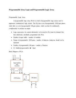
- 1. Programmable Array Logic and Programmable Logic Array Programmable Logic Array A programmable logic array (PLA) is a kind of programmable logic device used to implement combinational logic circuits. The PLA has a set of programmable AND gate planes, which link to a set of programmable OR gate planes, which can then be conditionally complemented to produce an output. Logic expressions for content information to be stored in PLA must be obtained first, then minimized, and finally programmed into PLA. Number of input buffer = number of variables Numer of programmable AND gates = number of minterms (minterms should not be repeated) Number of programmable OR gates = number of function X = fusible/programmable = fixed Block Diagram of PLA:
- 2. Application: One application of a PLA is to implement the control over a datapath. It defines various states in an instruction set, and produces the next state (by conditional branching). [e.g. if the machine is in state 2, and will go to state 4 if the instruction contains an immediate field; then the PLA should define the actions of the control in state 2, will set the next state to be 4 if the instruction contains an immediate field, and will define the actions of the control in state 4]. Programmable logic arrays should correspond to a state diagram for the system. Note that the use of the word "programmable" does not indicate that all PLAs are field- programmable; in fact many are mask-programmed during manufacture in the same manner as a mask ROM. This is particularly true of PLAs that are embedded in more complex and numerous integrated circuits such as microprocessors. PLAs that can be programmed after manufacture are called FPGA (Field-programmable gate array), or less frequently FPLA (Field- programmable logic array).. The Commodore 64 home computer released in 1982 used a "906114-01 PLA" to handle system signals. Example 1: Given the truth table, design the combinational circuit using PLA. A B C Y1 Y2 0 0 0 0 0 0 0 1 0 0 0 1 0 0 0 0 1 1 0 1 1 0 0 1 0 1 0 1 1 1 1 1 0 0 0 1 1 1 1 1 Solution: Y1:
- 3. 0 0 0 0 1 1 1 0 Y1= AB + AC Y2: 0 0 1 0 0 1 1 0 Y2= AC + BC Example 2: Given: Y1 = ABC + ABC + ABC Y2 = AB + AC + ABC Y3 = ∈ 0 ,2 , 6 ,7 Implement the given function into PLA. Y3:
- 4. 1 1 1 0 0 0 1 0 Y3= AC + AB
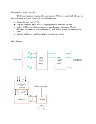
- 5. Programmable Array Logic (PAL) The PAL architecture consisted of a programmable AND array and a fixed OR array so that each output is the sum of a specific set of product terms. Commonly used type of PLD Only the connected inputs to AND are programmable, OR gates are fixed Unlike the PLA, a product term cannot be shared among two or more OR gates. Therefore, each function can be simplified by itself without regard to common product terms. Standard architecture used to implement combinational circuits Block Diagram:
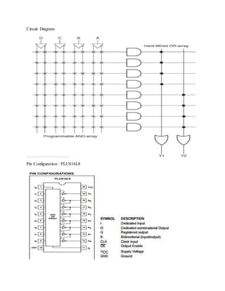
- 6. Circuit Diagram: Pin Configuration: PLUS16L8
- 7. Logic Diagram: PLUS16L8 Application: PAL’s also often have an extra circuitry connected to the output of OR gates is called Macrocell
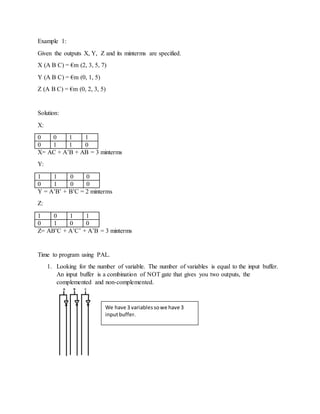
- 9. Example 1: Given the outputs X, Y, Z and its minterms are specified. X (A B C) = €m (2, 3, 5, 7) Y (A B C) = €m (0, 1, 5) Z (A B C) = €m (0, 2, 3, 5) Solution: X: 0 0 1 1 0 1 1 0 X= AC + A’B + AB = 3 minterms Y: 1 1 0 0 0 1 0 0 Y = A’B’ + B’C = 2 minterms Z: 1 0 1 1 0 1 0 0 Z= AB’C + A’C’ + A’B = 3 minterms Time to program using PAL. 1. Looking for the number of variable. The number of variables is equal to the input buffer. An input buffer is a combination of NOT gate that gives you two outputs, the complemented and non-complemented. We have 3 variablessowe have 3 inputbuffer.
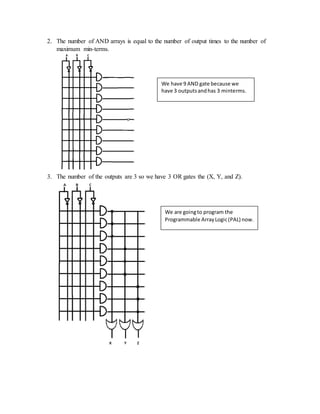
- 10. 2. The number of AND arrays is equal to the number of output times to the number of maximum min-terms. 3. The number of the outputs are 3 so we have 3 OR gates the (X, Y, and Z). We have 9 AND gate because we have 3 outputsandhas 3 minterms. We are goingto program the Programmable ArrayLogic(PAL) now.
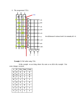
- 11. 4. The programmed PLA. Example 2. Full adder using PAL. In this example we are doing almost the same as we did to the example 1 but some changes occurred. A B Cin Sum Carry 0 0 0 0 0 0 0 1 1 0 0 1 0 1 0 0 1 1 0 1 1 0 0 1 0 1 0 1 0 1 1 1 0 0 1 1 1 1 1 1
- 12. K-Mapping Sum 0 1 0 1 1 0 1 0 Sum = AB’Cin’ + A’B’Cin + ABCin + A’BCin’ = 4 minterms Carry 0 0 1 0 0 1 1 1 Carry = ACin + BCin + AB = 3 minters Programming the PAL
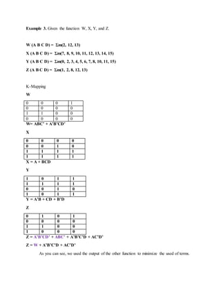
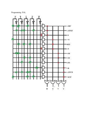
- 13. Example 3. Given the function W, X, Y, and Z. W (A B C D) = Σm(2, 12, 13) X (A B C D) = Σm(7, 8, 9, 10, 11, 12, 13, 14, 15) Y (A B C D) = Σm(0, 2, 3, 4, 5, 6, 7, 8, 10, 11, 15) Z (A B C D) = Σm(1, 2, 8, 12, 13) K-Mapping W 0 0 0 1 0 0 0 0 1 1 0 0 0 0 0 0 W= ABC’ + A’B’CD’ X 0 0 0 0 0 0 1 0 1 1 1 1 1 1 1 1 X = A + BCD Y 1 0 1 1 1 1 1 1 0 0 1 0 1 0 1 1 Y = A’B + CD + B’D Z 0 1 0 1 0 0 0 0 1 1 0 0 1 0 0 0 Z = A’B’CD’ + ABC’ + A’B’C’D + AC’D’ Z = W + A’B’C’D + AC’D’ As you can see, we used the output of the other function to minimize the used of terms.
- 14. Programming PAL.